
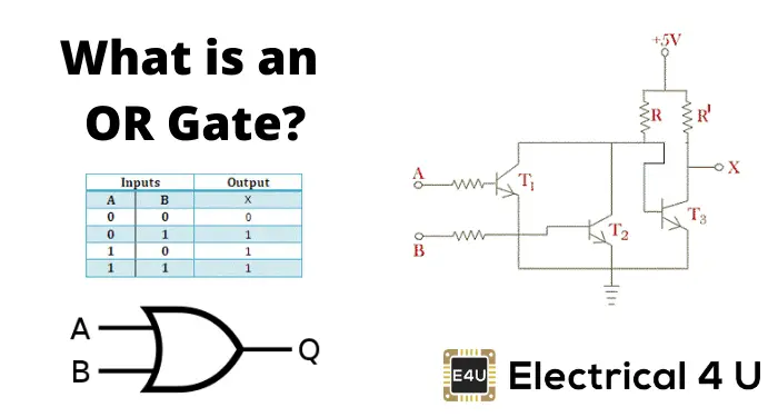
- OR Gate Definition: An OR gate is defined as a logic gate that outputs high (1) if one or both inputs are high (1).
- Working Principle: The working principle of an OR gate is to find the maximum between binary digits, resulting in a high output if any input is high.
- Truth Table: The truth table of an OR gate lists the output for all possible input combinations, showing how the gate responds.
- Diode Circuit: A diode can be used to create an OR gate, where any high input makes the output high.
- Transistor Circuit: Transistors can also form an OR gate, providing a high output if any transistor is switched on.
What is an OR Gate?
An OR gate is a logic gate that performs logical OR operation. A logical OR operation has a high output (1) if one or both the inputs to the gate are high (1). If neither input is high, a low output (0) results. Just like an AND gate, an OR gate may have any number of input probes but only one output probe.
The function of an OR gate is to find the maximum between two binary digits, while an AND gate finds the minimum.
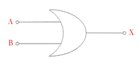
The logical symbol of 2 input OR gate is shown below:
OR Gate Truth Table
2 Input OR Gate
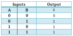
Truth tables list the output of a particular digital logic circuit for all the possible combinations of its inputs. The truth table of a 2 input OR gate can be represented as:
3 Input OR Gate
If instead of two inputs there are three inputs, this changes the logical symbol and truth table of the OR gate.
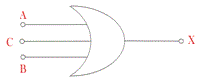
The logical symbol of a 3-input OR gate is represented as:
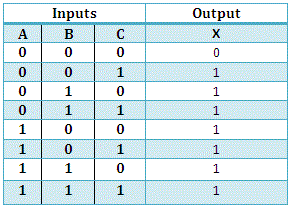
The truth table of a 3 input OR gate is:
In digital electronics, other logic gates include NOT gates, NAND gates, NOR gates, XOR gates, XNOR gates.
OR Gate Circuit Diagram
Like AND gate and OR gate can also be realized by using a diode or transistor circuit.
OR Gate Diode Circuit Diagram
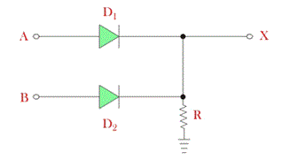
A simple two inputs OR gate can be realized by using a diode as follows,
In the circuit, if both inputs A and B are 0V, no voltage appears at X. If any input is +5V, the corresponding diode becomes forward biased and acts like a short circuit, making +5V appear at output X, which means logical 1.
Actually entire 5V will not appear at X, around 0.6 to 0.7 V will drop across the diode as forwarding bios voltage, and the rest of the voltage i.e. 5 – 0.6 = 4.4 V or 5 – 0.7 = 4.3 V will appear at X. This 4.4 V or 4.3 V is practically considered as logical 1.

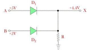
Now if both of the inputs are given with +5 V, both diodes will be forward biased. Hence, similarly, 4.4 V will appear at X.
Now if both of the inputs A and B are grounded or given 0V, There will be no voltage appears at X and hence X is considered as logical 0.
OR Gate Transistor Circuit Diagram
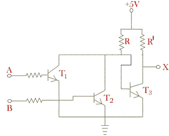
The OR gate can also be realized by using a transistor. In this case, the OR gate is referred to as the transistor OR gate. Two inputs such OR gate is shown below,
If both A and B are 0V, transistors T1 and T2 are off. The +5V supply cannot reach the ground through these transistors, so transistor T3 turns on. The +5V supply then flows to the ground through resistor R′ and transistor T3.
As the transistor T3 is in ON condition it will behave as ideally short circuited, hence the entire supply voltage + 5 V will drop across resistor Rʹ and X terminal (Node) will get 0V. In practice, transistor T3 will not be ideal short circuited it will have some voltage drop across it which will be around 0.6 – 0.7 V. This voltage will appear at node X, and this 0.6 or 0.7 volt is considered as logical 0.
Now, if the base terminal either of the transistors T1 or T2 or both are given with + 5 V, the respective transistor as both will be in ON condition. In that case, supply voltage + 5 V will get the path to ground through either of the transistors or both.
As a result, current starts flowing to the ground from supply through this path, and the entire supply voltage will drop across resistor R. So, the base of transistor T3 will not get sufficient potential to make the transistor T3 ON. Hence entire supply voltage will appear at X and the X becomes at a high logical state or logical 1.
OR Gate Integrated Circuits
OR gate is available in TTL and CMOS ICS, Where TTL is Transistor – Transistor Logic ICs and CMOS are Complementary MOSFET ICS. We will now discuss the arrangement of the OR gate on both the ICs.
In CMOS ICs the 4000 series is available. In digital electronic 4071 is the CMOS IC number of inputs in each gate is two. 4075 is 3 – input OR gate and 4072 is 4 – input OR gate in CMOS ICs. An internal gate picture of 4071 can help you understand this IC.
OR Gate IC 4071
4071 is a 14 pin 1C as you can see where four or gates are fixed together having two inputs. Pin number 14 is tvcc where maximum SV DC supply is given which activates the IC. Pin number 7 is grounded.

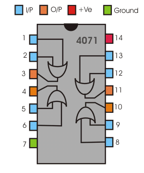
Pin 1 and 2 are the input for the first gate and 3 is the respective output for the first gate. Pin numbers 5 and 6 are inputs for the second gate whose output is pin number 4. For the third gate pin number 8 and 9 are the inputs whose output is pin number 10 for the last gate pin number 12 and 13 are the inputs whose respective output is at pin number 11. Thus how the IC looks internally for CMOS.
OR Gate IC 7432
In TTL logic the internal arrangement differs from that incase of CMOS logics. In TTL logic 2- input OR gate IC number is 74LS32. popularly known as 7432. LS stands for a low power schottky version.
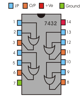
Again one more type of IC number is also available in the market which is 74HC32 where HC stands for high-speed CMOS version i.e. it has lower current consumption and wider voltage range. 74LVC32 is another low voltage CMOS version of the same. Let us have a discussion on 74LS32 which is a TTL IC. In this IC there are fourteen pins. The internal gate diagram of 7432 can make your idea clear.
In this IC, pin 1 and 2 are the inputs of the first gate where the output is from pin number 3. Again pin numbers 4 and 5 are the inputs of the second gate whose output is in pin 6. Pin 10 and 9 are the inputs of the fourth gate whose output is at pn 8. The input of the last gate or fourth gate is pin 13 and 12 and pin 11 is its output.
Pin 7 is ground and pin 14 is +vcc supply where again +Vcc supply where again +SVdC is the normal and maximum supply. One thing must be maintained at +SVDC. If the i/p voltage would be more than this it may cause damage to the IC.