
- MOSFET Definition: A MOSFET (Metal Oxide Semiconductor Field Effect Transistor) is defined as a capacitor-operated transistor device that controls current flow using voltage.
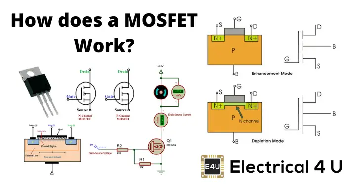
- Types of MOSFETs: MOSFETs come in four types: P-Channel and N-Channel in both Enhancement and Depletion modes, each with unique construction and operation.
- P-Channel Enhancement MOSFET: Uses a lightly doped n-type substrate and forms a conductive channel when a negative gate voltage is applied, allowing current flow.
- N-Channel Enhancement MOSFET: Utilizes a lightly doped p-type substrate and forms a conductive channel with a positive gate voltage, enabling current flow.
- Voltage Control: MOSFETs are voltage-controlled devices, meaning the gate voltage controls the current between the source and drain, a key concept in understanding mosfet electrical4u.
MOSFET stands for Metal Oxide Semiconductor Field Effect Transistor. The mosfet is a capacitor operated transistor device. The capacitor plays an essential role for operating a MOSFET. We also call the device as Insulated Gate Field Effect Transistor (IGFET) or Metal Insulator Field Effect Transistor (MIFET). Why we call so we will understand when we look into the constructional features of this transistor device. We must take a look into the construction of MOSFET while going through the working principle of mosfet. Construction wise we can categorise the device into four types.
- P – Channel Enhancement MOSFET
- N – Channel Enhancement MOSFET
- P – Channel Depletion MOSFET
- N – Channel Depletion MOSFET
P – Channel Enhancement MOSFET
We also call the p channel MOSFET as PMOS. Here, a substrate of lightly doped n-type semiconductor forms the main body of the device. We usually use silicon or gallium arsenide semiconductor material for this purpose. Two heavily doped p-type regions are there in the body separated by a certain distance L. We refer this distance L as channel length and it is in order of 1 µm. Now there is a thin layer of silicon dioxide (SiO2) on the top of the substrate. We may also use Al2O3 for the purpose but SiO2 is most common. This layer on the substrate behaves as a dielectric. There is an aluminum plate fitted on the top of this SiO2 dielectric layer.
Now the aluminum plate, dielectric and semiconductor substrate form a capacitor on the device. 
The terminals connected to two p-type regions are the source (S) and drain (D) of the device respectively. The terminal projected from the aluminum plate of the capacitor is gate (G) of the device. We also connect the source and body of the mosfet to earth to facilitate the supply and withdrawal of free electrons as per requirement during operation of the MOSFET.  Now let us apply a negative voltage at gate (G). This will create negative static potential at the aluminum plate of the capacitor. Due to capacitive action, positive charge gets accumulated just below the dielectric layer.
Basically, the free electrons of that portion of the n-type substrate get shifted away due to the repulsion of negative gate plate and consequently layers of uncovered positive ions appear here. Now if we further increase the negative voltage at the gate terminal, after a certain voltage called threshold voltage, due to the electrostatic force, covalent bonds of the crystal just below the SiO2 layer start breaking. Consequently, electron-hole pairs get generated there. The holes get attracted and free electrons get repealed due to the negativity of the gate. In this way, the concentration of holes increases there and create a channel of holes from source to drain region. Holes also come from both heavily doped p-type source and drain region. Due to the concentration of holes in that channel the channel becomes conductive in nature through which electric current can pass.  Now let us apply a negative voltage at drain terminal. The negative voltage in the drain region reduces the voltage difference between gate and drain reduces, as a result, the width of the conductive channel get reduced toward the drain region as shown below. At the same time, current flows from source to drain shown by arrowhead.
 The channel created in the mosfet offers a resistance to the current from source to drain. The resistance of the channel depends on the cross-section of the channel and the cross section of the channel again depends on the applied negative gate voltage. So we can control the current from the source to drain with the help of an applied gate voltage hence MOSFET is a voltage controlled electronic device. As the concentration of holes forms the channel, and the current through the channel gets enhanced due to increase in negative gate voltage, we name the MOSFET as P – Channel Enhancement MOSFET.
N – Channel Enhancement MOSFET
Working of N – Channel Enhancement MOSFET is similar to that of P – Channel Enhancement MOSFET but only operationally and constructionally these two are different from each other. In N Channel Enhancement MOSFET a lightly doped p-type substrate forms the body of the device and source and drain regions are heavily doped with n-type impurities. Here also we connect the body and source commonly to the ground potential. Now, we apply a positive voltage to the gate terminal. Due to positivity of the gate and corresponding capacitive effect, free electrons i.e. minority carriers of the p-type substrate get attracted towards the gate and form a layer of negative uncovered ions there just below the dielectric layer by recombining these free electrons with holes. If we continually increase the positive gate voltage, after the threshold voltage level, the recombinations process gets saturated and then free electrons start to accumulate at the place to form a conductive channel of free electrons. The free electrons also come from the heavily doped source and drain n-type region. Now if we apply a positive voltage at the drain, current start flowing through the channel. The resistance of the channel depends on the number of free electrons in the channel and the number of free electrons in the channel again depends on the gate potential of the device. As the concentration of free electrons forms the channel, and the current through the channel gets enhanced due to increase in gate voltage, we name the MOSFET as N – Channel Enhancement MOSFET. 
N – Channel Depletion MOSFET
The working principle of depletion MOSFET is a little bit different from that of enhancement MOSFET. N – Channel Depletion MOSFET the substrate (body) is of p-type semiconductor. The source and drain regions are of the heavily doped n-type semiconductor. The space between source and drain regions is diffused by n-type impurities. Now if we apply a potential difference between source and drain, a current starts flowing through the entire n region of the substrate.  Now, let us apply a negative voltage at the gate terminal. Due to the capacitive effect, the free electrons get repealed and shifted downward in the n region just below the SiO2 dielectric layer. As a result, there will be layers of positive uncovered ions below the SiO2 dielectric layer. In this way, there will be a depletion of charge carriers occurred in the channel and hence the overall conductivity of the channel gets reduced. In this situation, for the same applied voltage at the drain, the drain current gets reduced. Here we have seen that we can control the drain current by varying depletion of charge carriers in the channel and hence we call it as depletion MOSFET. Here, the drain is in a positive potential, the gate is in a negative potential and the source is at zero potential. So the voltage difference between drain to gate is more than that of source to gate, hence the width of the depletion layer is more towards drain than that towards the source.
P – Channel Depletion MOSFET
Cotructionwise a p channel depletion MOSFET is just reverse of the n channel depletion MOSFET. Here the prebuild channel is made of p – type impurities in between heavily doped p – type source and drain region. When we apply a positive voltage at the gate terminal, due to electrostatic action, minority carriers i.e. free electrons of the p-type region get attracted and form static negative impurity ions there. Hence a depletion region gets formed in the channel and consequently, the conductivity of the channel gets reduced. In this way, by applying the positive voltage at gate we can control the drain current. 