

- JFET Definition: A Junction Field Effect Transistor (JFET) is a semiconductor device that controls electrical current using an applied voltage.
- Types of JFETs: There are two main types: n-channel and p-channel, each using different charge carriers (electrons or holes) and having opposite operating polarities.
- Operation Mechanism: The JFET operates by altering the width of the depletion layer via gate voltage, which affects the channel’s conductivity and the overall current flow.
- Application in Electronics: JFETs are commonly used in circuits as amplifiers and switches due to their high impedance and efficient current control.
- Unique Properties: The device features high input impedance and no gate current under ideal conditions, making it a robust component for various electronic applications.
A Junction Field Effect Transistor (JFET) is a semiconductor device within the field effect transistor family. It operates via an electric field across its junction. This article focuses on the JFET, one of the two main types of field effect transistors, the other being the Metal Oxide Semiconductor Field Effect Transistor (MOSFET). JFET is a voltage control device whereas BJT is a current control device. The current through JFET is caused due to the flow of majority carriers whereas in BJT flow of current is due to both majority and minority carriers. Since only majority carriers are involved in creations of current in JFET, it is a unipolar device. The input impedance of a JFET is very high.
Types of JFET
There are two types of JFETs: n-channel and p-channel, each designed for specific circuit applications.
N Channel JFET
An n channel JFET is made of Si or GaAs bar. The bar is doped with n-type impurities. One metallic terminal is attached to each of both ends of the bar. One of the terminals is called drain terminal, and the other is called the source terminal. Two sides of the bar are highly doped with p-type impurities. The region which doped with p-type impurities is called gate region. A metallic terminal is connected to the gate region, and the terminal is called the gate terminal. 
P Channel JFET
Similarly, a p channel JFET is made of Si or GaAs bar doped with p-type impurities. The sides of the bar are highly doped with n-type impurities. Here also the drain, and the source terminal are connected to two ends of the bar. The terminal attached to the side n-type region is the gate terminal.
NB:- Here in both types of junction field effect transistor both drain and source terminal can be interchangeable.
Applying a voltage between the drain and source terminals initiates current flow. This current moves through the channel—a space between two oppositely doped regions—carried by the drift of majority carriers from the source to the drain terminal.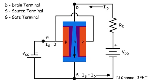
Under normal conditions, the n-channel JFET’s drain terminal has a positive potential, while the p-channel’s has a negative one. The gate voltage creates a reverse bias in the PN junction between the gate and the channel, allowing control over the depletion layer’s width—and thus the channel opening—by adjusting the gate voltage. If by changing the gate terminal voltage, the width of the depletion layer increases, it is extended into the channel and reduces the opening of the channel and therefore the current through the channel gets decreased. Hence we can conclude that by controlling gate voltage we can control the drain current. Depending on that typical property of the JFET we can use this JFET for many different electronic applications. A JFET can be used as a switch, as an amplifier etc.
Properties of JFET
- This is a voltage control device since the current through the channel gets controlled by gate voltage. In other words, the electric field across the junction effects the operation of the transistor and that is why it is named as junction field effect transistor.
- As in normal operating condition, the junction between input gate region and channel remains to reverse biased, the input impedance of the transistor is high.
- Ideally, there will be no gate current in JFET.
- Majority carriers only contribute the current through the channel in the device, i.e., free electrons in n channel and holes in p channel and these are the reason why a transistor is called unipolar device.