

- Transistor Biasing Definition: Transistor biasing is the process of setting the DC operating voltage or current of a transistor to ensure proper function and amplification of AC input signals.
- Purpose of Biasing: Ensuring a transistor operates correctly, transistor biasing adjusts current and voltage levels, vital for its performance in amplification and switching roles.
- Types of Biasing Circuits: Some common types include Fixed Base Bias, Collector Feedback Bias, and Voltage Divider Bias, each offering different stability and performance characteristics.
- Stability Factors: The stability of a transistor’s operation in biasing circuits is crucial, with some circuits like the Voltage Divider Bias providing high thermal stability and reducing performance fluctuations due to temperature changes.
- Biasing for Different Transistors: While the discussed biasing techniques primarily focus on Bipolar Junction Transistors (BJTs), similar methods are applicable to Field Effect Transistors (FETs), highlighting the versatility of biasing principles.
What is Transistor Biasing?
Transistor Biasing is the process of setting a transistor’s DC operating voltage or current conditions to the correct level so that any AC input signal can be amplified correctly by the transistor.
Transistors are one of the most widely used semiconductor devices which are used for a wide variety of applications, including amplification and switching. However, to achieve these functions satisfactorily, a transistor must be supplied with a certain amount of current and/or voltage.
The process of setting these conditions for a transistor circuit is referred to as transistor biasing. Transistor biasing can be accomplished by various techniques that give rise to different kinds of biasing circuits.
However, all of these circuits are based on the principle of providing the right amount of base current, IB, and, in turn, the collector current, IC from the supply voltage, VCC when no signal is present at an input.
Moreover, it is crucial to select the collector resistor, RC, appropriately. This ensures the collector-emitter voltage, VCE, stays above 0.5V for germanium transistors and 1V for silicon transistors. Several biasing circuits are detailed below.
The types of transistor biasing include:
- Fixed Base Bias or Fixed Resistance Bias
- Collector Feedback Bias
- Dual Feedback Bias
- Fixed Bias with Emitter Resistor
- Emitter Bias
- Emitter Feedback Bias
- Voltage Divider Bias
Types of Transistor Biasing
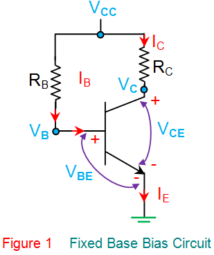
Fixed Base Bias or Fixed Resistance Bias
In this circuit, the base-emitter junction is forward biased by the voltage drop across RB, caused by the base current, IB, flowing through it. The corresponding mathematical expression for IB is shown in the figure.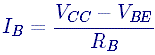
Here the values of VCC and VBE are fixed, while the value for RB is constant once the circuit is designed.
This configuration ensures a constant IB, establishing a fixed operating point—hence the name, fixed base bias. However, this type of biasing has a stability factor of (β+1), which contributes to lower thermal stability.
The reason behind this is the fact the β-parameter of a transistor is unpredictable and varies up to a large extent, even in the case of a transistor with the same model and type. This variation in β results in large changes in IC, which cannot be compensated by any means in the proposed design.
Hence, this kind of β dependent bias is prone to the changes in operating points brought about by the variations in transistor characteristics and temperature.
However, it is to be noted that fixed base bias is most simple and uses fewer components. Moreover, it offers the chance for the user to change the operating point anywhere in the active region by changing the value of RB in the design.
Furthermore, it offers no load on the source as there is no resistor across the base-emitter junction. Due to these factors, this kind of biasing is used in switching applications and to achieve automatic gain control in the transistors.
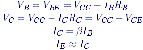
Here, the expressions for other voltages and currents are given as
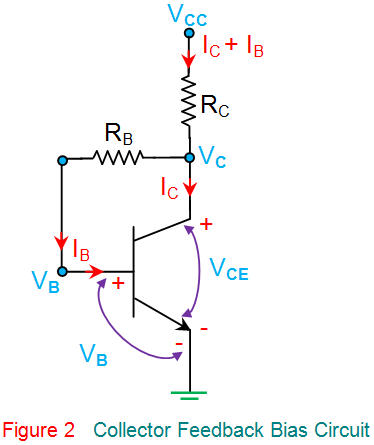
Collector Feedback Bias
In this circuit (Figure 2), the base resistor RB is connected across the collector and the base terminals of the transistor.
This means that the base voltage, VB, and the collector voltage, VC are inter-dependent because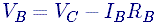
Where,
From these equations, it is seen that an increase in IC decreases VC, which results in a reduced IB, automatically reducing IC.
This design ensures the Q-point, or operating point, remains stable despite variations in the load current, keeping the transistor in its active region, independent of β value.
Furthermore, this circuit is also referred to as a self-biasing negative feedback circuit as the feedback is from output to input via RB.
This kind of relatively simple bias has a stability factor that is less than (β+1), which results in better stability when compared to fixed bias.
However, the action of reducing the collector current by base current leads to a reduced amplifier gain.
Here, other voltages and currents are expressed as
Dual Feedback Bias
Figure 3 shows a dual feedback bias network which is an improvisation over the collector feedback biasing circuit as it has an additional resistor R1 which increases the stability of the circuit.
This is because an increase in the current flow through the base resistors results in a network resistant to the variations in the values of β.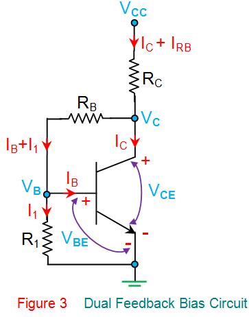
Here, 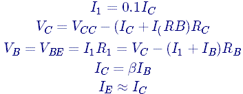
Fixed Bias with Emitter Resistor
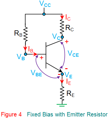
As evident from Figure 4, this biasing circuit is nothing but a fixed bias network with an additional emitter resistor, RE.
Here, if IC rises due to an increase in temperature, the IE also increases, increasing the voltage drop across RE.
This results in the reduction of VC, causing a decrease in IB, bringing IC back to its normal value. Thus, this kind of biasing network offers better stability compared to a fixed base bias network.
However, including RE lowers the amplifier’s voltage gain due to unwanted AC feedback. The circuit includes mathematical equations for various voltages and currents, as follows: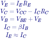
Emitter Bias
This biasing network (Figure 5) uses two supply voltages, VCC and VEE, equal but opposite in polarity.
Here VEE forward biases the base-emitter junction through RE while VCC reverse biases the collector-base junction. Moreover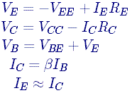
In this kind of biasing, IC can be independent of both β and VBE by choosing RE >> RB/β and VEE >> VBE, respectively, which results in a stable operating point.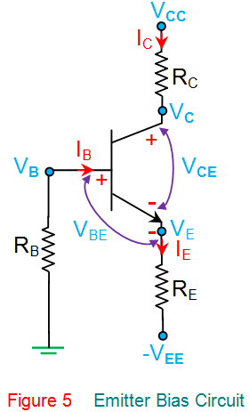
Emitter Feedback Bias
This kind of self-emitter bias (Figure 6) employs both collector-base feedback and emitter feedback to result in higher stability. Here, the emitter-base junction is forward biased by the voltage drop occurring across the emitter resistor, RE due to the flow of emitter current, IE.
An increase in the temperature increases IC, causing an increase in the emitter current, IE. This also leads to an increase in the voltage drop across RE which decreases the collector voltage, VC, and in turn IB, thereby bringing back IC to its original value.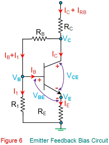
However, this results in a reduced output gain due to degenerative feedback, which is nothing but unwanted AC feedback, wherein the amount of current flowing through the feedback resistor is determined by the value of the collector voltage, VC.
This effect can be compensated by using a large bypass capacitor across the emitter resistor, RE. The expressions corresponding to various voltages and currents in this low-power-supply-voltage suitable biasing network are given as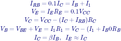
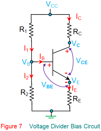
Voltage Divider Bias
This type of biasing network (Figure 7) employs a voltage divider formed by the resistors R1 and R2 to bias the transistor.
This means that the voltage developed across R2 will be the base voltage of the transistor, which forward biases its base-emitter junction. In general, the current through R2 will be fixed to be 10 times the required base current, IB (i.e., I2 = 10IB).
This is done to avoid its effect on the voltage divider current or the changes in β. Further, from the circuit, one gets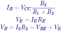
In this kind of biasing, IC is resistant to the changes in both β as well as VBE, which results in a stability factor of 1 (theoretically), the maximum possible thermal stability.
As IC increases due to a temperature rise, IE increases, causing an increase in the emitter voltage VE, reducing the base-emitter voltage VBE. This results in the decrease of base current IB, which restores IC to its original value.
The higher stability offered by this biasing circuit makes it most widely used despite providing a decreased amplifier gain due to the presence of RE.
Apart from the analyzed basic types of biasing networks, Bipolar Junction Transistors (BJTs) can also be biased using active networks or by using either silicon or Zener diodes.
Furthermore, it is also to be noted that although the biasing circuits are explained for BJTs, similar bias networks also exist in the case of Field Effect Transistors (FETs).