

- PISO Shift Register Definition: A PISO shift register is defined as a device that loads data in parallel format and retrieves it serially.
- Basic Components: A PISO shift register includes control lines, combinational circuits, flip-flops, and clock and clear pins.
- Loading Data: When the control line is low, input data is loaded in parallel through activated gates into the register.
- Shifting Data: With the control line high, data shifts right by one bit with each clock pulse, and it takes n clock cycles to get the entire n-bit data serially.
- Left-Shift Option: By modifying the design, data can be shifted from right to left, creating a left-shift PISO shift register with the same basic working principle.
In Parallel In Serial Out (PISO) shift registers, the data is loaded onto the register in parallel format while it is retrieved from it serially. Figure 1 shows a PISO shift register which has a control-line  and combinational circuit (AND and OR gates) in addition to the basic register components (flip-flops) fed with clock and clear pins.
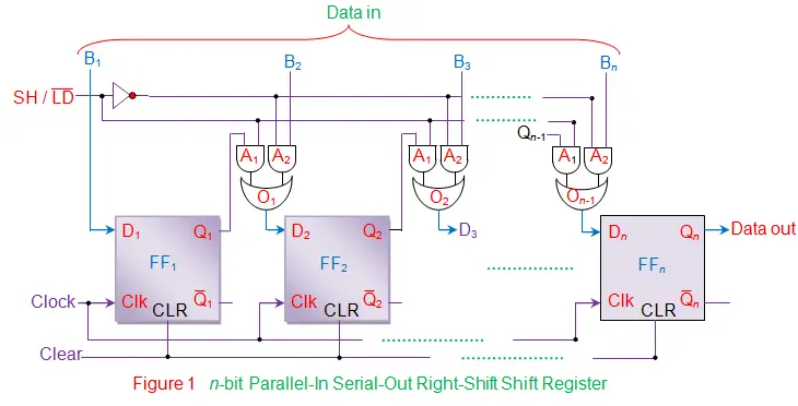
Here  control line is used to select the functionality of the shift register amongst shift or load at a given instant of time. This is because when the line is made low, A2 AND gates of all the combinational circuits become active while A1 gates become inactive.
Thus the bits of the input data word (Data in) appearing as inputs to the gates A2 are passed on as the outputs of OR gates at each individual combinational circuit. This causes the individual bits of the Data in to be loaded/stored into respective flip-flops at the appearance of first leading edge of the clock (except the bit B1 which gets directly stored into FF1 at the first clock tick). This indicates that all the bits of the input data word are stored into the register components at the same clock tick.
Next, line is driven high to activate the gates A1 of the combinational circuits which inturn disables the gates A2. This causes output bit of each flip-flop to appear at the output of the OR gate driving the very-next flip-flop (except the last flip-flop FFn) i.e. output bit of FF1 (Q1) appears as the output of OR gate 1 (O1) connected to D2; Q2 = output of O2 = D3 and so on. At this stage, if the rising edge of the clock pulse appears, then Q1 appears at Q2, Q2 appears at Q3, … and Qn-1 appears at Qn.
This process shifts the data stored in the register to the right by one bit. With each clock pulse, one bit exits the PISO shift register through the nth flip-flop’s output pin (Data out = Qn of FFn), forming the serial output. It takes n clock cycles to retrieve the entire n-bit input data word serially.
The truth table of the PISO shift register emphasizing the loading and retrieval processes is shown by Table I, while the corresponding wave forms are shown by Figure 2.
By modifying the design of Figure 1, data bits can shift from right to left, creating a left-shift PISO shift register (Figure 3). However, the basic working principle remains the same.