- NOT Gate Definition: A NOT gate, also known as an inverter, is a basic digital logic gate that produces an output which is the opposite of its input.
- Symbol and Truth Table: The symbol for a NOT gate reflects its function of inverting the input signal, with a truth table confirming its consistent output inversion.
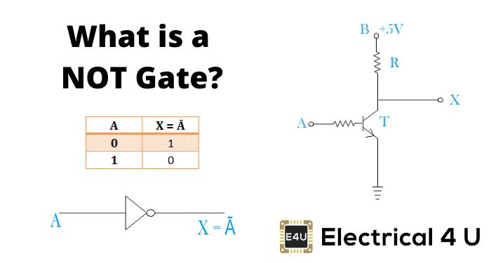
- Circuit Diagram: A simple bipolar transistor setup demonstrates the NOT gate’s working principle, where it inverts the input signal.
- Working Principle: The NOT gate operates by using a transistor to switch the electrical path based on the input; high input results in low output and vice versa.
- Practical Output Understanding: Practical Output Understanding
What is a NOT Gate?
A NOT gate, also called an inverter, flips its digital input signal: it outputs high (logical 1) when the input is low (logical 0) and vice versa. This action distinguishes it from power inverter, despite the similar name. The symbol for a NOT gate demonstrates this inversion.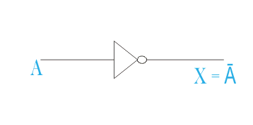
In a NOT gate, if the input variable is labeled A, the output will be Ā, where Ā is the inverse of A. This relationship is denoted by a bar over the letter (−). For example, if A is 1, then Ā equals 0, and if A is 0, then Ā equals 1.
Truth tables list the output of a particular digital logic circuit for all the possible combinations of its inputs. The truth table of a NOT gate can be represented as: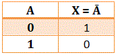
Besides the NOT gate, there are several other types of logic gates: AND gates, OR gates, NAND gates, NOR gates, XOR gates, XNOR gates, each with unique functions and uses in digital circuits.
NOT Gate Transistor Circuit Diagram
A NOT gate can easily be realized by using a simple bipolar transistor. The transistor circuit diagram of a NOT gate (also known as a transistor inverter) is shown below: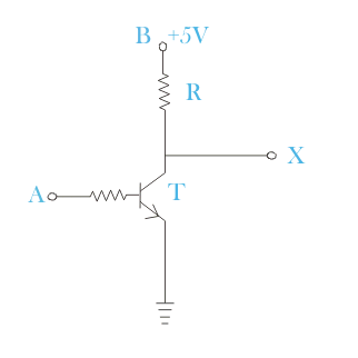
The transistor diagram above will be used to demonstrate how a NOTE gate works.
How a NOT Gate Works
Let us examine the above transistor circuit when a high input voltage is applied, i.e. +5V.
In this condition, the transistor T gets enough base potential to make it ‘ON’.
Once the transistor is ON, the supply voltage (+5V) finds a path to the ground through the resistor R. Ideally, the transistor behaves as if it’s short-circuited, causing almost all the supply voltage to drop across R. Consequently, no voltage appears at output X, resulting in a low output. However, practically, there’s a small voltage drop across the transistor’s collector and emitter, even when it’s ON.
This collector-emitter voltage is about 0.6V. So, at the above-said input condition, the entire supply voltage +5V will not drop across the resistor instead it will be 5 – 0.6 = 4.4V. So, 0.6V is practically considered as logical zero or low.
Now let us examine the condition, where input A = 0V i.e. base terminal of the transistor is given with 0V or grounded.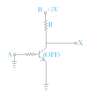
At that condition, as the base of the transistor is at 0 potential, the transistor T will be in OFF condition and hence, the supply voltage will not get any path to the earth and the entire supply voltage will appear at the output terminal of the NOT gate high or logical 1, when input terminal A is low or logical zero.
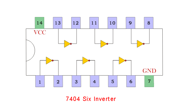
NOT Gate IC
The IC available at the market for NOT gate is IC 7404. One 7404 IC contains a total of six transistors inverter or simply six NOT gate.