

- Conductivity Definition: The conductivity of a semiconductor is defined as its ability to conduct electricity, which is moderate due to its intermediate free electron concentration.
- Role of Electrons and Holes: In semiconductors, both free electrons and holes act as charge carriers, enabling electrical conduction.
- Temperature Effects: Conductivity of semiconductors increases with temperature because higher temperatures generate more free electrons and holes.
- Energy for Bond Breaking: The energy needed to break covalent bonds in semiconductors, releasing electrons and creating holes, is crucial for understanding their conductivity.
- Applications of Conductivity: The temperature sensitivity of semiconductors is useful for creating devices like thermistors that measure temperature changes
It is well known to us that the conductivity of a material depends on the concentration of free electrons in it. Good conductors consist large concentration of free electrons whereas insulators consist small concentration of free electrons. These conductors have a high conductance value (and hence a low resistance value). The concentration level of the free electron in semiconductors is in between the values of density of free electrons in conductor and insulator.
This is why the conductivity of a semiconductor is moderate—not very high or very low. In semiconductors, valence electrons are not free like in metals; they are trapped in bonds between adjacent atoms. Germanium and silicon are commonly used semiconductors, and their crystal structures consist of a repeating three-dimensional unit.
For example, each germanium atom has 32 electrons orbiting its nucleus.
Each atom in the germanium contributes four valence electrons to make the covalent bond with four adjacent germanium atoms in the crystal. So the atoms are tetravalent. The inert ionic core of the germanium acts as a positive charge of +4 electronic charges. The valance electrons in germanium crystal serve to bind one atom to the next.
Hence, it can be said that the valance electrons are tightly bounded with the atoms in the crystal. Because of that, although a germanium atom has four valence electrons in it germanium crystal as a whole is not an excellent conductor of electricity. At absolute zero temperatures a semiconductor crystal behaves just like an insulator as there are no free carriers of electricity available.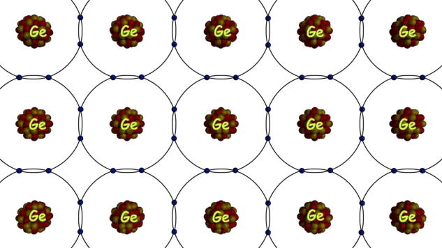
However, at room temperature (300oK), some covalent bonds in the crystal break due to available energy, releasing free electrons and allowing the semiconductor to conduct electricity to some extent.
The energy needed to break a covalent bond is about 0.72 eV in germanium and 1.1 eV in silicon at room temperature. When a covalent bond breaks, one electron leaves the bond, creating a vacant spot called a hole.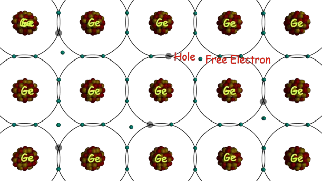
The significance of hole in the semiconductor is that they can also be referred as a carrier of electricity compared to electrons. The mechanism by which the holes carry electricity is somewhat different from the mechanism by which electrons carry electricity.
When there is an incomplete bond in a semiconductor crystal, a hole exists in the bond. It is a little bit easier for the electron, to form a bond with neighborhood atoms; hence, it leaves its previous position for occupying the newly created hole nearby. When an electron moves to fill a hole from its previous position in the bond, it leaves another new hole behind it.
When the second hole is created, then electron of any other neighborhood bond may come out to fill up the second hole with creating a new hole behind it. Hence, it can be visualized that as such holes are moving in the direction opposite to the movement of electrons. In this way semiconductor conducts electricity with help of these two types of electricity or charge carriers (electrons and holes).
From the above explanation if we sincerely think we can visualize that while a hole moves from one direction to other direction at the same time electron moves in just opposite direction of that. It means whenever holes move in a respective forward direction, the negative charge moves in the opposite or backward direction.
Negative charge moves in backward direction imply that the positive charge was moving in forward direction. Hence, it can be concluded that the movement of a hole involves for carrying a positive charge in a semiconductor crystal. In an ideal semiconductor crystal number of holes created per unit time is exactly equal to the number of electrons becomes free during this time.
If the temperature increases the rate of creation of electron-hole pair increases and when the temperature decreases, number electron – hole pairs is reduced due to recombination of electrons and holes in the crystal.
When one electron-hole pair is created, there are two charge carriers produced. One is negative charge carrier associated with the electron and other is positive charge carrier associated to the hole.
Say the mobility of the hole in the crystal is μh and the mobility of electron in the same crystal is μe. These holes and electrons move in opposite direction. The electrons always tend to move in opposite to the applied electric field, the current density due to drift of holes is given by,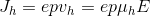
The current density due to drift of electrons is given by,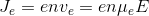
As the drifting of holes contributes current in the same direction and drifting of electrons provides current in opposite direction, in both cases, currents are in the same direction that is in the direction of drifting of holes. Hence, resultant current due to these both charge carriers will be arithmetic sum of two currents and hence resultant current density would be,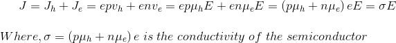
Where, n is the magnitude of free electron concentration, ‘p’ is the magnitude of hole concentration and σ is the Conductivity of Semiconductor.
If the semiconductor is ideally pure, then there would be the same number of free electrons and holes. That means n = p = ni (say). If the temperature of the semiconductor increases, the concentration of charge carriers (electrons and holes) is also increased. Hence, the conductivity of a semiconductor is increased accordingly. The relation between temperature and concentration of charge carrier in a pure or intrinsic semiconductor is given as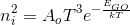
Where, T is the temperature in Kelvin Scale.
From the above equation, it is found that the concentration of charge carriers in a semiconductor exponentially increases very rapidly with the increase of temperature. Here we find that the concentration of hole and electrons in germanium increases 6% for an increase of every degree centigrade in temperature.
It is of 8% for silicon. This phenomenon makes a semiconductor device much sensitive to temperature. This change of concentration of charge carriers in a semiconductor due to temperature effects on characteristics and performance of semiconductor devices. Hence special care is to be taken to maintain the temperature within a specified limit during operation of this type of semiconductor devices.
Although, this prompt sensitivity to variation of temperature makes the semiconductor useful for many applications. Many specially made semiconductors are used as the transducers for measuring temperature. These devices are known as thermistors.