

- Semiconductor Physics Definition: Semiconductor physics is defined as the study of materials with electrical conductivity between conductors and insulators, primarily involving elements like silicon and germanium.
- Properties of Semiconductors: Semiconductors have moderate resistivity and a negative temperature coefficient of resistance, meaning their resistance decreases with increasing temperature.
- Covalent Bonding: In semiconductors, each atom forms four covalent bonds with neighboring atoms, creating a stable crystal structure.
- Energy Band Theory: Semiconductors have a small energy gap between the valence and conduction bands, allowing electrons to move and conduct electricity when energy is applied.
- Types of Semiconductors: Intrinsic semiconductors are pure, while extrinsic semiconductors are doped with impurities to increase conductivity, forming n-type and p-type semiconductors.
The Physics of a Semiconductor
Semiconductor atoms have four valence electrons, giving them unique electrical properties. This makes them useful in electronic components like diodes, transistors, and SCRs. They are called semiconductors due to their moderate electrical conductivity.
The resistivity of a semiconductor ranges from 10– 4 Ω – m to 0. 5 Ω – m. Where the resistivity of copper is about 1.7 × 10– 8 Ω – m in room temperature and resistivity of glass is about 9 × 10¹¹ Ω – m. Copper is good conductor and glass is insulater.
We have already told that semiconductor is useful in electronic circuit elements not only because of its moderate resistivity but because of its many other special properties.
Some main properties of semiconductors are,
- The resistivity is less than an insulator and more than a conductor.
- The temperature coefficient of resistance is negative.
- When impurities are added to a semiconductor, the resistivity of the semiconductor changes abruptly.
Bonds in Semiconductor
The valence electrons in semiconductor atoms take a vital role in bonding between atoms in the semiconductor crystal. Bonding between atoms occurs because each atom has a tendency to feel its outer most cell with eight electrons.
Each semiconductor atom has four valence electrons and can share four electrons from neighboring atoms to complete eight electrons in its outermost shell. This sharing of electrons creates covalent bonds.
Each semiconductor atom creates four covalent bonds with four neighbouring atoms in the crystal. That means, one covalent bond is created with each of four neighbouring semiconductor atom. The figure below shows the covalent bonds formed in a germanium crystal.
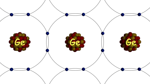 In germanium crystal, each atom has eight electrons in its last orbit. But in an isolated single germanium atom, there are 32 electrons. The first orbit consists of 2 electrons. The second orbit consists of 8 electrons. The third orbit consists of 18 electrons and rests 4 electrons are in fourth or outer most orbit.
But in a germanium crystal, each atom shares 4 valence electrons from four neighbouring atoms to fill its outermost orbit with eight electrons. In this way, each of them in the crystal will have eight electrons in its outermost orbit. 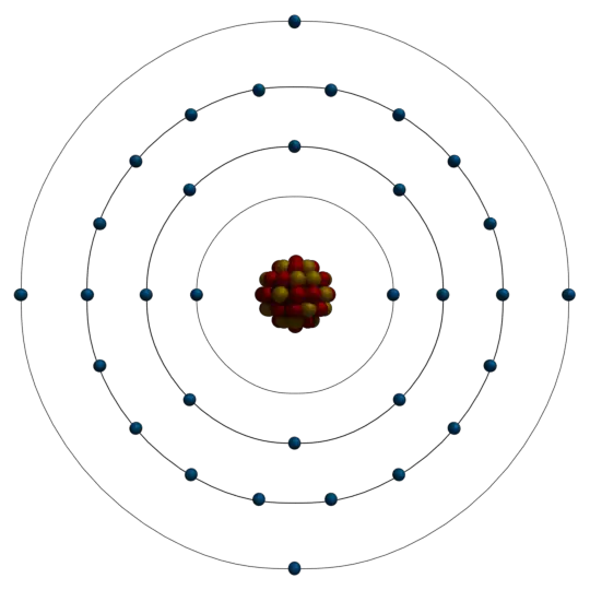
Forming covalent bonds associates each valence electron with an atom, leaving no free electrons in an ideal semiconductor crystal. The atoms are orderly arranged due to these bonds, creating the crystal structure of a semiconductor.
Commonly Used Semiconductor
There are many semiconductors but few of them are used for electronic circuits. Two most commonly used semiconductors are silicon and germanium. The silicon and germanium require lower energy to break their covalent bonds in the crystal. This is the main reason for using these two semiconductors most commonly. Silicon requires 1.1 eV for breaking any covalent bond in its crystal and germanium requires
0.7 eV for the same purpose.
Silicon
Silicon has total 14 electrons in its isolated atom. The first orbit consists of 2 electrons. The second orbit consists of 8 electrons and the third orbit consists of 4 electrons. As there are four electrons in the outer most orbit of a silicon atom, the silicon is a tetravalent element.
Each silicon atom in silicon crystal creates covalent bonds with four neighbouring silicon atoms. In this way, each atom of a silicon crystal gets 8 electrons in its outermost orbit. The atom to atom covalent bonds arrange the silicon atoms in the crystal in an orderly manner.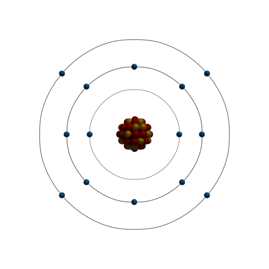
Germanium
Germanium has 32 electrons in its isolated atom. The first, second and third orbit of the germanium atom consists of 2, 8, 18 electrons respectively. The fourth or outermost orbit of the germanium consists of [32 – (2+8+18) = 4] 4 electrons.
In the similar way of silicon atoms in the crystal, germanium atoms in germanium crystal make four covalent bonds with four adjacent germanium atoms. For same reasons as in the silicon crystal, germanium atoms in germanium crystal arrange themselves in an orderly manner.
Energy Band Theory of Semiconductor
In a semiconductor crystal, the valence band is filled with valence electrons due to covalent bonds between atoms.
Hence, in ideal condition, the entire conduction band is empty. But the typicality about the semiconductor is that the band gap between conduction band and valence band is moderately small. It is about 1 eV. Hence, for any external energy supplied to the crystal, the electrons of valence band can acquire an ability to migrate to the conduction band and increase the conductivity.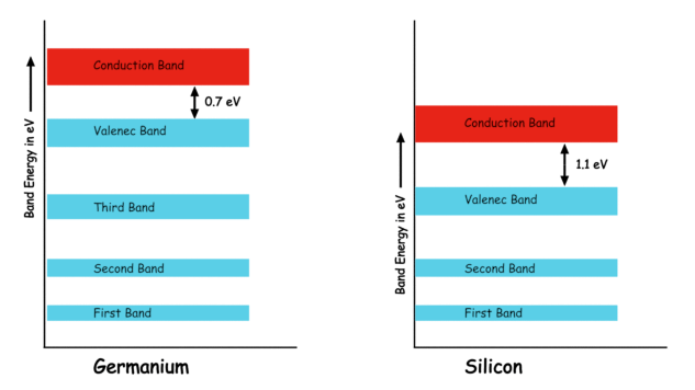
We call the energy gap between conduction and valence as forbidden energy gap. The forbidden energy gap of silicon is 1.1 eV and same for germanium is 0.7 eV. As the forbidden energy gap is quite moderate, an electron in valence band requires a small energy to cross the forbidden energy gap to become free. Even at room temperature, there are numbers of free electrons available in a silicon or germanium semiconductor crystal. Not only in silicon or germanium semiconductor, in all other semiconductors there are numbers of free electrons at room temperature, because of the same reason. These free electrons, which are in conduction bands, cause the conductivity of semiconductor. Although there are numbers of free electrons in a semiconductor at room temperature, but still the number is quite small compared to number of atoms in a piece of semiconductor crystal. It is found that, at room temperature out of 1010 semiconductor atoms, there will be only one free electrons.
Because of these small number of free electrons, the semiconductors possess moderate conductivity i.e. not as good as metallic conductor and not as poor as the insulator. At absolute zero temperature, there will be no external energy available in a semiconductor crystal. There will be no valence electron crossing the forbidden energy gap. Hence, there will be no free electron available in the semiconductor crystal. Consequently, the semiconductor will behave as a perfect insulator at absolute zero temperature.
Now when the temperature of the semiconductor rises from absolute zero, the electrons of valence band get energy and cross the forbidden gap, hence becomes free electrons. As the temperature rises continually, the number of free electrons gets increased in the semiconductor crystal and therefore the conductivity of the semiconductor increases.
The conductivity is the inverse of resistance. That means, with an increase in temperature, the resistance of a semiconductor decreases. Hence, we can say a semiconductor has the negative temperature coefficient of resistance. Hence, at a room temperature, if we apply a potential difference across a semiconductor, there will be a small current flowing through the semiconductor because of its moderate conductivity developed in the semiconductor at room temperature.
Whenever there will be an electron migrated from valence band to conduction band, a vacant place in created in the valence band, where a new electron can sit. We refer this vacant place in valence band where an electron can sit, as a hole.
As soon as an electron becomes free, there will be a hole created behind it in the valence band. Hence for each free electron in a pure semiconductor, there will be a hole. Hence we can say, any external energy, mainly thermal energy creates not only free electrons in the semiconductor crystal rather it creates electron-hole pairs.
Each covalent bond in the semiconductor, consists of two valence electrons contributed by two neighbouring atoms. When one of the valence electrons leaves the bond, the bond becomes incomplete. This incomplete bond has a strong tendency to complete itself by attracting an electron. The hole is the electron vacancy created in the covalent bond and as this hole can attract electron, we can assume the hole as an equivalent of positive charge. But there is no physical existence of positive charge but till it can act as a positive charge. In other words, a hole in the semiconductor is a virtual positive charge.
Like free electrons, holes in the semiconductor crystal move from one point to other. But the movement of holes in the semiconductor is different from that of free electrons. The free electrons move physically in the semiconductor crystal structure. The holes move in the semiconductor crystal virtually.
Each hole created in the crystal is strongly associated with its parent atoms. Hence, physically it does not move. When an electron from other covalent bond comes and sits on the hole, the hole vanishes. But the electron sitting on the hole coming from any other covalent bond hence the electron has created a hole in its previous bond. So, a new hole has already appeared there. In this way, one hole vanishes and another hole appears at the same time. Virtually as such a hole moves from its old position to its new position.
When we apply a potential difference across a semiconductor, free electrons move from negative to the positive side of the potential. At the same time holes move from positive side negative side.
Intrinsic Semiconductor
Intrinsic semiconductor is extremely pure semiconductor. At room temperature, electron-hole pairs created in the intrinsic semiconductor crystal only due to thermal excitation. An intrinsic semiconductor does have a moderate conductivity of electricity due to the concentration of free electrons and holes thermally created in the crystal, at room temperature.
Extrinsic Semiconductor
We can change the conductivity of the semiconductor significantly by adding some impurities in it. We refer to the process of adding impurities in a semiconductor for changing its conductive property, as doping.
Added impurities in the semiconductor either increase the number of free electrons or increase the number of holes depending upon the type of impurities added. When we add pentavalent elements as impurities, the number of free electrons in the extrinsic semiconductor crystal increases.
When we add trivalent elements as impurities the number of holes in the semiconductor increase. We call, the extrinsic semiconductor with more number of free electrons than holes as n-type semiconductor. We call the extrinsic semiconductor with more number of holes than the number of free electrons, as p-type semiconductor. So the amount of dopping determines the conductivity of the semiconductor. The type of dopped elements determines the type of semiconductor whether it is n-type or p-type in nature.
N-type and P-type Semiconductor
When we add pentavalent impurity elements to an intrinsic semiconductor material, it becomes an n-type semiconductor. Addition of pentavalent eliminates contributes a large number of free electrons in the semiconductor. We commonly use arsenic and
antimony as the pentavalent impurity for the purpose.
Let us take a pure germanium. The pure germanium will have some free electrons as well as holes at room temperature. There are two reasons due to which free electrons and holes always present even in a pure semiconductor crystal.
1) At room temperature, there would be some thermally generated electron-hole pairs.
2) We can not prepare absolute pure materials practically. Hence there are always some impurities present in the semiconductor although the quantity of there impurity may be negligibly small. Among this impurities, there may be pentavalent and trivalent impurities. These pentavalent and trivalent impurities create free electrons and holes in the semiconductors even without any external doping of impurities.
Now let us add a pentavalent element like arsenic in that germanium semiconductor. The arsenic has five valence electrons since it is pentavalent. The four of the valence electrons of each arsenic atoms take part in the creation of covalent bonds with four neighbouring germanium atoms. In this way, each arsenic atom fills its valence band.
The Fifth electron of the arsenic which does not take part in the formation of the covalent bond, cannot get the place in the valence bond. This electron then migrates to the conduction band of the crystal and becomes free electron. In this way, there will be many free electrons intentionally created by adding pentavalent impurities in the semiconductor.
Now the total number of free electrons (n) in the germanium would be, the sum of thermally created free electrons (Na) free electrons created due to inherent impurities of the semiconductor (Nb) and free electrons created due to externally added pentavalent impurities (Nc).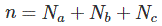
Now the total number of holes (p) in the semiconductor would be the sum of the thermally created hole (Pa) and holes created due to inherent impurities of the semiconductor (Pb).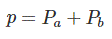
The externally added pentavalent impurity ideally do not contribute any hole to the semiconductor. Again, the number of externally added or dropped impurity atoms (here it is arsenic ) is quite large hence the number of free electrons in the pentavalent dopped semiconductor is quite larger than the number of holes.
Because of the larger number of free electrons in the semiconductor, we call the semiconductor as negative – type or n type semiconductor. Same explanation can be applied to the positive type or p type semiconductor.