- PIPO Shift Register Definition: A PIPO shift register is a type of storage device where data loading and retrieval happen in parallel at a single clock pulse.
- Data Handling: Both the input and output of data in a PIPO shift register occur simultaneously, enabling efficient data management.
- Modification for Shifting: To convert a basic PIPO register into a PIPO shift register, additional combinational circuits and control lines are added.
- Right-shift Operation: By activating certain control lines, a PIPO shift register can shift data bits to the right, demonstrating its dynamic functionality.
- Educational Figures: The use of figures and tables in the article visually explains how data shifts within the register, aiding comprehension.
Parallel In Parallel Out (PIPO) shift registers are the type of storage devices in which both data loading as well as data retrieval processes occur in parallel mode. Figure 1 shows a PIPO register capable of storing n-bit input data word (Data in). Here each flip-flop stores an individual bit of the data in appearing as its input (FF1 stores B1 appearing at D1; FF2 stores B2 appearing at D2 … FFn stores Bn appearing at Dn) at the instant of first clock pulse. Further, at the same instant, the bit stored in each individual flip-flop also appears at their respective output pins (Q1 = D1; Q2 = D2 … Qn = Bn). This indicates that both data storage as well as data recovery occur at a single (and at the same) clock pulse in PIPO registers.
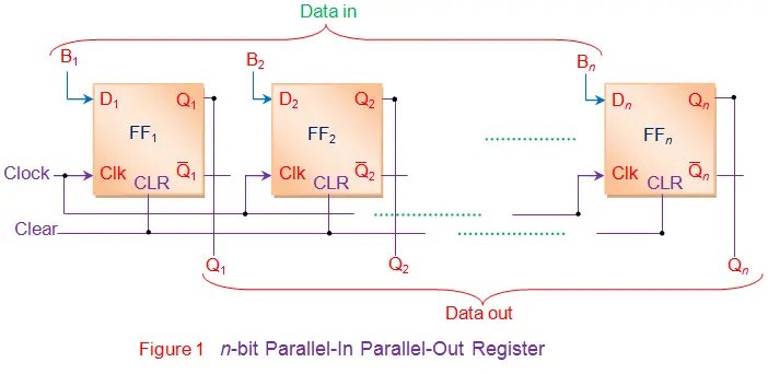
It’s important to note that the PIPO register shown in Figure 1 cannot shift data bits. To convert this PIPO register into a PIPO shift register, you must modify its circuit by adding combinational circuits and control lines, as illustrated in Figure 2.
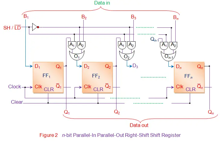
When the control line goes low, the A2 AND gates in all combinational circuits activate, while the A1 gates become inactive.
The input data bits (Data in) that enter the A2 gates are transmitted as outputs from the OR gate and are then stored into their corresponding flip-flops at the first leading edge of the clock pulse. The exception is the bit B1, which is directly stored into FF1 right at the first clock pulse. This indicates that all the bits of the input data word are stored into the register components at the same clock tick. At the same time, these bits also appear at the output pins of the respective flip-flops thus yielding parallel-output data word at the same clock tick.
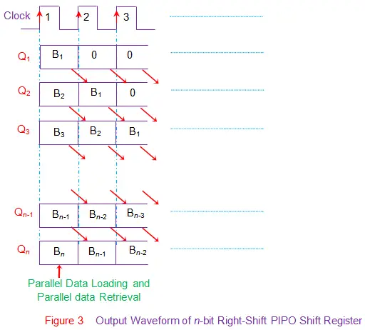
Additionally, when the control line is set high, the A1 gates in all combinational circuits are enabled, while the A2 gates are disabled. This causes the output bit of each flip-flop to appear at the output of the OR gate driving the very-next flip-flop (except the last flip-flop FFn) i.e. output bit of FF1 (Q1) appears as the output of OR gate 1 (O1) connected to D2; Q2 = output of O2 = D3 and so on. At this stage, if the rising edge of the clock pulse appears, then Q1 appears at Q2, Q2 appears at Q3, … and Qn-1 appears at Qn. This is nothing but right-shift of the data stored within the register by one-bit. This working is further emphasized in the Table I and Figure 3.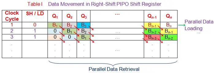
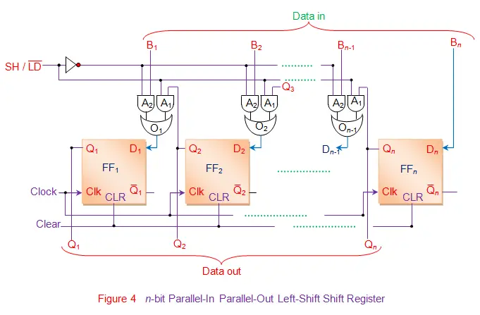
Similar to the right-shift PIPO shift register, there can also be a left-shift PIPO shift register as shown by Figure 4. Nevertheless the mode of working remains the same.