

- Voltage Regulator 7805 Definition: The 7805 voltage regulator is defined as a fixed linear regulator that provides a stable +5V DC output from an input voltage between 7V and 35V.
- PIN Configuration: The 7805 has three pins: an input pin for unregulated voltage, a ground pin for 0V, and an output pin for regulated 5V.
- Heat Dissipation: Excess energy is released as heat, requiring proper heat sinks to prevent malfunction and ensure efficiency.
- Internal Components: The internal block diagram includes an error amplifier, Zener diode, transistors, and SOA protection to stabilize and control the voltage.
- Applications: The 7805 voltage regulator is used in phone chargers, UPS systems, and other devices needing a reliable 5V power supply.
Voltage sources often have fluctuations and cannot provide a fixed output. To ensure a constant and steady output, voltage regulators are used. These integrated circuits, known as voltage regulator ICs, help manage voltage. Let’s focus on the IC 7805.
The 7805 voltage regulator is part of the 78xx series of voltage regulator ICs. It is a fixed linear regulator, where “xx” represents the fixed output voltage. For the 7805, it provides a +5V DC regulated power supply. It also includes a provision for a heat sink. The input voltage can go up to 35V, and the IC maintains a constant 5V output for any input below this threshold.
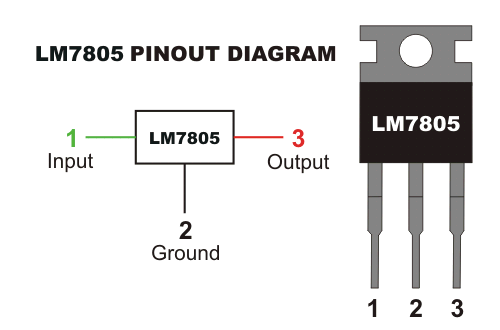
PIN 1-INPUT
The function of this pin is to give the input voltage. It should be in the range of 7V to 35V. We apply an unregulated voltage to this pin for regulation. For 7.2V input, the PIN achieves its maximum efficiency.
PIN 2-GROUND
We connect the ground to this pin. For output and input, this pin is equally neutral (0V).
PIN 3-OUTPUT
This pin is used to take the regulated output. It will be 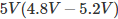
Heat Dissipation in IC 7805
In the 7805 voltage regulator, much energy is lost as heat. The heat comes from the difference between input and output voltage. If this difference is large, more heat is generated. Without a proper heat sink, this excess heat can cause malfunction.
The minimum tolerable difference between the input and output voltage to maintain proper output is called dropout voltage. It’s best to keep the input voltage 2 to 3V higher than the output voltage, or use a suitable heat sink to dissipate excess heat. Proper calculation of the heat sink size is crucial.
Now, we can analyze the relation of generated heat and the input voltage value in this regulator with the following two examples.
Assume a system with input voltage 16V and required output current be 0.5A.
So, heat generated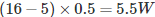
Thus, 5.5W heat energy is wasted and the actual energy used 
That is almost double energy is wasted as heat.
Next, we can consider the case when input is lower, say 9V.
In this case, heat generated 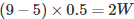
From this, we can conclude that for high input voltage, this regulator IC will become highly inefficient. If you’d like to learn more, we have a large range of free digital electronics MCQ questions.
Internal Block Diagram of 7805 Voltage Regulator
The internal block diagram of IC 7805 is represented in the figure below:
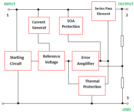
The block diagram comprises of an error amplifier, series pass element, current generator, reference voltage, current generator, starting circuit, SOA protection and thermal protection.
The operational amplifier functions as an error amplifier, while the Zener diode provides the reference voltage.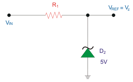
Transistor is the series pass element here. It is used for dissipating additional energy in the form of heat. It controls the output voltage by controlling the current among the input and output. SOA is the Safe Operating Area. It is in fact the conditions of voltage and current in which the equipment is expected to work without any self-damage. Here for the SOA protection, bipolar transistor is implemented with a series resistor and an auxiliary transistor. Heat sink is implemented for thermal protection when there is high supply voltage.
Regulated Power Supply Circuit
The voltage regulator 7805 and the other components are arranged in the circuit as shown in figure.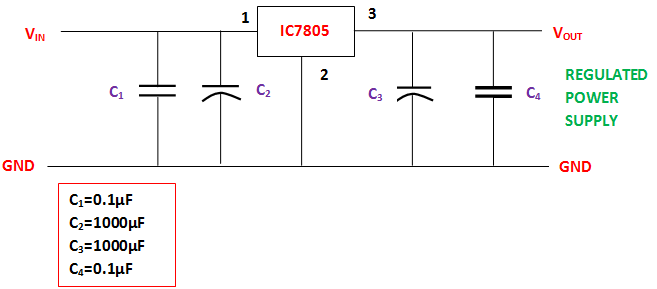
The purposes of coupling the components to the IC7805 are explained below.
C1– It is the bypass capacitor, used to bypass very small extent spikes to the earth.
C2 and C3– They are the filter capacitors. C2 is used to make the slow changes in the input voltage given to the circuit to the steady form. C3 is used to make the slow changes in the output voltage from the regulator in the circuit to the steady form. When the value of these capacitors increases, stabilization is enlarged. But these capacitors single-handedly are unable to filter the very minute changes in the input and output voltages.
C4– like C1, it is also a bypass capacitor, used to bypass very small extent spikes to the ground or earth. This is done without influencing other components.
Applications of Voltage Regulator 7805 IC
- Current regulator
- Regulated dual supply
- Building circuits for Phone charger, UPS power supply circuits, portable CD player etc
- Fixed output regulator
- Adjustable output regulator etc.