
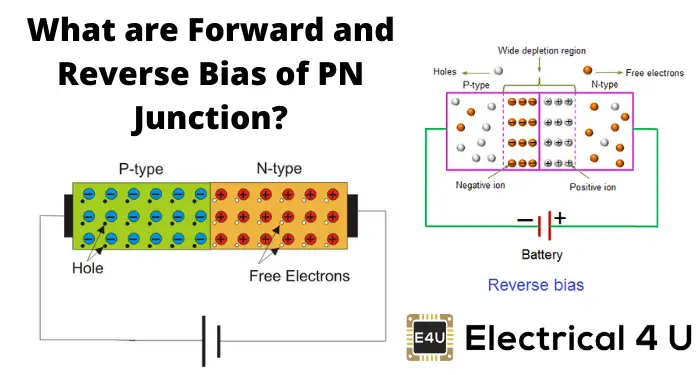
- PN Junction Diode Definition: A PN junction diode is defined as a semiconductor device that allows current to flow in one direction in forward bias and blocks current in reverse bias.
- Forward Bias: In forward bias, the p-type region is connected to the positive terminal and the n-type to the negative terminal, reducing the depletion layer and allowing current flow.
- Reverse Bias: In reverse bias, the p-type region is connected to the negative terminal and the n-type to the positive terminal, increasing the depletion layer and preventing current flow.
- Current Behavior: In forward bias, current flows easily once the depletion layer is reduced. In reverse bias, only a minimal current flows due to minority carriers.
- Breakdown Conditions: High reverse voltage can cause breakdowns (Zener or Avalanche), leading to a sharp increase in current, which is crucial in understanding diode operation limits.
Forward Biased PN Junction
A PN junction is said to be forward-biased when the p-type region of a junction is connected to the positive terminal of a voltage source and the n-type region is connected to the voltage source’s negative terminal.
In forward bias, electrons in the p-type material are attracted to the positive terminal, breaking covalent bonds and moving towards the terminal.
This breaks more covalent bonds, increasing the electron concentration near the terminal, where electrons recombine with holes.
Holes increase in the p-type region away from the junction and decrease near the terminal as they move from the terminal to the junction.
With more holes near the negative ions layer, electrons recombine with holes, creating new holes and reducing the layer’s width until it vanishes.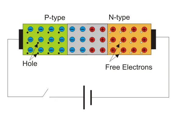
Similarly, due to the negative terminal of the source, the free electrons in the n-type region will repeal towards the junction where they will find the layer of positive impurity ions and start recombine with these ions and generate free electrons inside the layer. Consequently, the width of positive impurity ions is reduced, and finally, it vanishes.
In these ways, both layers of ions disappear, and there will be no more depletion layer. After the depletion layer disappeared, free electrons from the n-type region can easily drift to the p-type region and holes from the p-type region to the n-type region in the crystal.
Hence, ideally, there will be no obstruction of flowing current, and the PN junction behaves as the short circuit.
Reverse Biased PN Junction
A PN junction is in reverse bias when the positive terminal connects to the n-type region and the negative terminal connects to the p-type region.
When there is no voltage applied across the p n junction, the potential developed across the junction is 0.3 volts at 25oC for germanium on the junction and 0.7 volts at 25oC for silicon p n junction.
The polarity of this potential barrier is the same as the voltage source’s polarity applied during the reverse biased condition. If the reverse biased voltage across the PN junction is increased the barrier potential developed across the PN junction is also increased. Hence, the PN junction is widened.
When positive terminal of the source is connected to the n-type region, the free electrons of that region are attracted towards the positive terminal of the source because of that more positive impurity ions are created in the depletion layer which makes the layer of positive impurity ions thicker.
At the same time since the negative terminal of the source is connected to the p-type region of the junction, electrons are injected in this region.
Due to the positive potential of the n-type region, the electrons are drifted towards the junction and combine with holes adjacent to the layer of positive impurity ions and create more positive impurity ions in the layer. Hence, the thickness of the layer increases.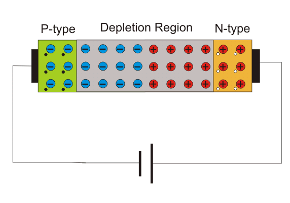
In this way, the overall width of the depletion layer increases along with its barrier potential. This increment of the depletion layer’s width will continue till the barrier potential reaches to applied reverse biased voltage.
Although this increment of barrier potential will continue up to applied reverse-biased voltage, if the applied reverse biased voltage is sufficiently high, then the depletion layer will disappear due to Zener breakdown and avalanche breakdowns.
It is also to be noted that after completion of reverse biased depletion layer there is no more drift of charge carriers (electrons and holes) through the junction as the potential barrier opposes the applied voltage which has the same value as the potential barrier.
Although tiny current flow from n-type region to p-type region due to minority carriers that are thermally generated electrons in p-type semiconductor and holes in an n-type semiconductor.
Forward Current in PN Junction
When the battery voltage is applied across the forward bias junction, a current will flow continuously through this junction.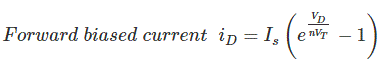
IS is Saturation Current (10-9 to 10-18 A)
VT is Volt-equivalent temperature (= 26 mV at room temperature)
n is the Emission coefficient (1 ≤ n ≤ 2 for Si ICs)
Actually, this expression is approximated.
Reverse Current in PN Junction
When a p-n junction is connected across a battery in such a manner that its n-type region is connected to the positive potency of the battery and the p-type region is connected to the negative potency of the battery the p n junction is said to be in reverse biased condition. Ideally, there is no current flowing through the junction. But practically there will be a tiny reverse bias current iD which is expressed as.
iD drops to zero value or minimum value. iD can be written as i0.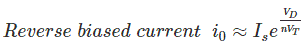
IS is Saturation Current (10-9 to 10-18 A)
VT is Volt-equivalent temperature (= 26 mV at room temperature)
n is the Emission coefficient (1 ≤ n ≤ 2 for Si ICs)
Actually, this expression is approximated.
General Specification of PN Junction
A p-n junction is specified in four manners.
- Forward Voltage Drop (VF): Is the forward biasing junction level voltage (0.3V for Germanium and 0.7V for Silicon Diode )
- Average Forward Current (IF): It is the forward-biased current due to the drift electron flow or the majority carriers. If the average forward current exceeds its value, the diode gets overheated and may be damaged.
- Peak Reverse Voltage (VR): The maximum reverse voltage across the diode at its reverse biased condition. Over this reverse voltage diode will go for breakdown due to its minority carriers.
- Maximum Power Dissipation (P): It is the product of the forward current and the forward voltage.
V-I Characteristics of A PN Junction
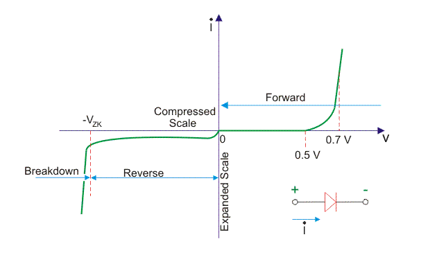
In the forward bias, the operational region is in the first quadrant. The threshold voltage for Germanium is 0.3 V and for Silicon is 0.7 V. Beyond this threshold voltage, the graph goes upward in a non-linear manner. This graph is for the dynamic Resistance of the junction in the forward bias.
In the reverse bias the voltage increases in the reverse direction across the p-n junction, but no current due to the majority carriers, only a minimal leakage current flows. But at a certain reverse voltage p-n junction breaks in conduction.
It is only due to the minority carriers. This amount of voltage is sufficient for these minority carriers to break the depletion region. In this situation, a sharp current will flow through this junction. This breakdown of voltage is of two types.
- Avalanche Breakdown: it is not a sharp graph, rather inclined linear graph, i.e. after the break down a small increase in reverse voltage causes more sharp current gradually.
- Zener Breakdown: This breakdown is sharp and no need to increase reverse bias voltage to get more current, because current flows sharply.
Resistances of p-n Junction
Dynamic Resistance of p-n Junction
From V-I characteristics of a p-n junction, it is clear that graph is not linear. The forward biased p-n junction resistance is rd ohm; it is called AC resistance or dynamic resistance. It is equivalent to the slope of voltage-current of the PN junction.
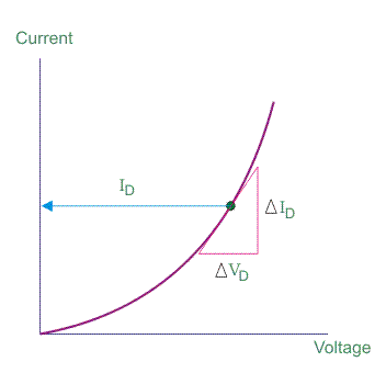
Average AC Resistance of p-n Junction
Average AC resistance is determined by the straight line drawn linking the intersection of the minimum and maximum values of the external input voltage.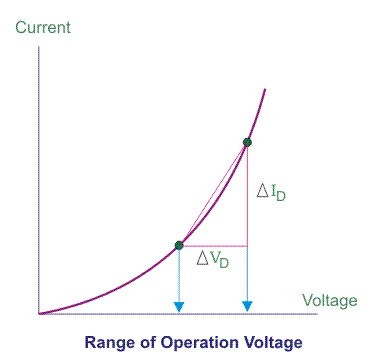
Some important terms related to p-n Junction
Transition Capacitance of PN Junction
When the depletion region exists in the common junction around, the diode acts as a capacitor. Here the depletion region is the dielectric and two regions (p-type and n-type) at both ends act as the charged plates of a capacitor. As the depletion layer decreases, the capacitance value goes down.
Diffusion Capacitance of PN Junction
It the capacitance of the diode in the forward biased condition and it is defined as the ratio of transiting charge created to the differential change in voltage.
When the current through the junction increases the diffusion capacitance also increases. Along with this increase in current, the forward-biased resistance also decreases. This diffusion capacitance is somewhat greater than the Transition capacitance.
Storage Time of PN Junction
It is the time taken by the electrons to move from the n-type region to the p-type region and p-type region to the n-type region by applying simultaneous forward and reverse bias voltage during switching.
Transition Time of PN Junction
It is the time taken by the current to decrease to reverse leakage current. This transition time can be determined by the geometry of P-N junction and concentration of the doping level.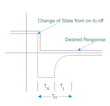
Reverse Recovery Time of P-N Junction
It is the sum of the storage time and transition time. It is the time for a diode to raise applied current to get 10% of the constant state value from the reverse leakage current.