- Clamper Circuit Definition: A clamper circuit is an electronic device that modifies the DC level of a signal to set its peak values to a desired level without changing its peak-to-peak amplitude.
- Component Functionality: The basic components of a clamper circuit include a diode, capacitor, and resistor, each playing a crucial role in the function of the circuit.
- Time Constant Importance: The time constant in clamper circuits is vital, as it should be large enough to prevent significant discharge of the capacitor during non-conductive phases of the diode.
- Operation of Clampers: Positive and negative clamper circuits adjust the DC level of an input signal either upward or downward, depending on the orientation of the diode.
- Circuit Types: There are both biased and unbiased versions of clamper circuits that can provide different levels of DC shift to the output signal based on the specific requirements of the application.
What is a Clamper Circuit?
A clamper circuit, or clamping circuit, fixes the positive or negative peak values of a signal to a defined level by adjusting the signal’s DC value. This circuit type does not alter the peak-to-peak values but shifts the entire signal up or down to the desired level.
Clamper circuits are also known as Baseline Stabilizers, DC Reinserters, Level Shifters, or D.C Restorers, terms that more clearly describe their function.
Clamper circuits will add the DC element, positive or negative, to the AC input signal. It pushes the signal towards the positive or the negative side (as shown in the figures below).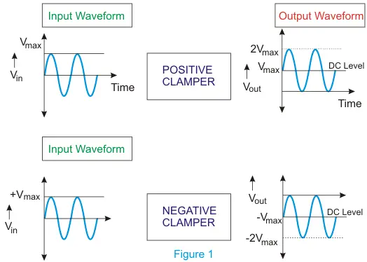
Here, when it shifts the signal to the upward or positive sides, both the negative peak and the zero levels will meet, which is called the positive clamper circuit (top part of the above figure).
When it shifts the signal to the downside or negative side, both the positive peak and the zero levels will meet, which we refer to as the negative clamper circuit (bottom part of the above figure).
A basic clamper circuit includes three components: a capacitor, a resistor, and a diode. Sometimes, an additional DC supply is necessary for extra shifting.
The nature of the waveform remains the same, but the difference is in the shifted level (up or down). The peak to the peak value of the waveform will never change.
The peak value and average value of the input waveform and the clamped output will be different. The time constant of the circuit (RC) must have to be ten times the time period of the entering (input) AC voltage for the better clamping action.
Let’s look at a diode negative clamper, shown in figure 2 below.
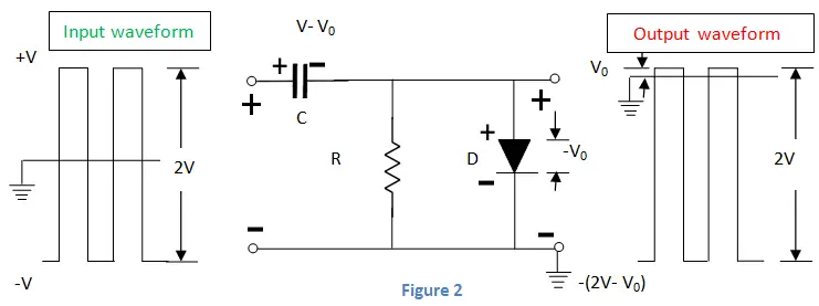
Throughout the positive half cycle of input, the D diode will conduct, and the output voltage will be the same as the barrier potential of the diode (V0).
At that time, the capacitor will get charged to (V – V0). Throughout the negative half cycle of input, the diode will become negative biased, and it has no role on capacitor voltage. The capacitor cannot discharge a lot because of the high value of R.
Therefore, the output voltage will be – (2V- V0). The peak-to-peak voltage will be 2V. The output waveform that we get will be the original signal shifted in the downward direction.
Next, let’s look at a positive diode clamper shown in figure 3 below. The only distinction from the previous circuit is that diode is in reverse polarity. So the output will be the shifted original signal in the upward direction.
Its underlying function is the same as the negative clamper circuit above the clamper circuit.
This time though, the diode is pointing in the upward direction, not downwards. This means that the current is now flowing in the opposite direction.
Thus we can conclude that we obtain the positive clamper if the diode in the circuit points in the upward direction, and we get a negative camper when the diode points in the downward direction.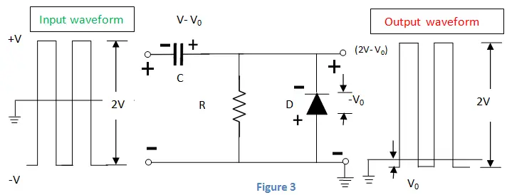
How Does a Clamping Circuit Work?
In general, the clamper circuit depends on a variation in the capacitor time constant. 
The time constant should be sufficient that the capacitor voltage does not discharge considerably throughout the non-conducting diode period.
Select capacitance and resistance values to maintain a high time constant, using high resistance to prevent the capacitor from discharging quickly.
All through the diode conducting period, the capacitor charging should be high-speed. For this, we select a small value of capacitance.
The C in the positive clamper charges quickly throughout the first negative phase of AC input voltage. When Vin becomes +ve, the C serves as a voltage doubler, and when Vin is –ve, the C operates as a battery with voltage Vin.
Thus, we can conclude that the capacitor and input voltage act against each other. This results in zero net voltage as seen by the load.
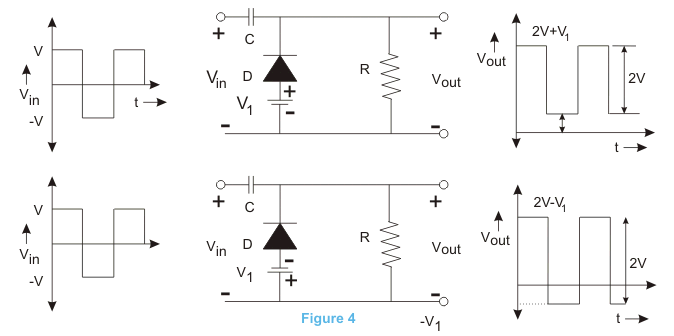
Figures 4 and 5 illustrate the biased positive and biased negative clamping circuits, respectively.