
- Power Diode Definition: A power diode is defined as a diode used in power electronics circuits, designed to handle higher currents than regular diodes.
- N- Layer Importance: The N- layer in power diodes is lightly doped, increasing the space charge region thickness and allowing higher reverse-biased voltages.
- V-I Characteristics: Power diodes show a linear increase in forward current due to higher ohmic resistance, differing from the exponential increase in regular diodes.
- Reverse Recovery Time: Reverse recovery time is the time it takes for the reverse current to decay to 25% of its peak value after the diode is switched off.
- Softness Factor: The softness factor of power diodes is the ratio of charge removal times from the semiconductor and depletion regions, indicating voltage transients upon turn-off.
What is a Power Diode?
A power diode is defined as a diode used in power electronics circuits, capable of handling higher currents than regular diodes. It has two terminals and conducts current in one direction, with a construction designed for higher power applications.
To understand power diodes better, let’s revisit how a standard diode works. A diode is defined as the simplest semiconductor device, with two layers, two terminals, and one junction.
Ordinary signal diodes have a junction formed by a p type semiconductor and n type semiconductor. The lead joining the p-type is called the anode, and the lead joining the n-type is called the cathode.
The figure below depicts the structure of an ordinary diode and its symbol.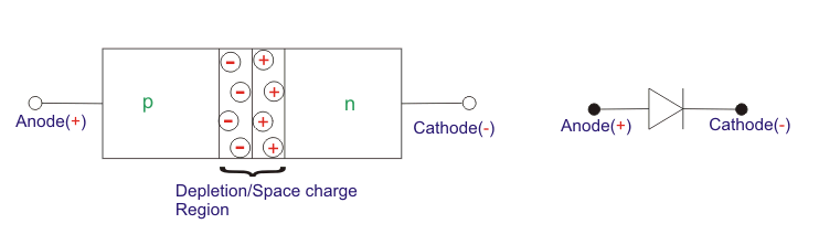
Power diodes are also similar to regular diodes, although they vary slightly in their construction.
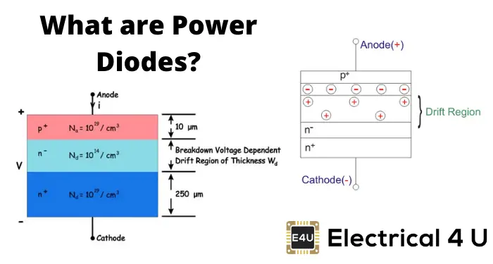
In regular diodes (also known as “signal diode”), the doping level of both P and N sides is the same and hence we get a PN junction, but in power diodes, we have a junction formed between a heavily doped P+ and a lightly doped N– the layer which is epitaxially grown on a heavily doped N+ layer. Hence the structure looks as shown in the figure below.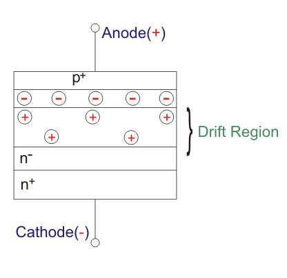
The N– layer is the key feature of the power diode which makes it suitable for high power applications. This layer is very lightly doped, almost intrinsic and hence the device is also known as a PIN diode, where i stands for intrinsic.
As we can see in the figure above that the net charge neutrality of the space charge region is still maintained as was the case in the signal diode but the thickness of the space charge region is quite high and deeply penetrated into the N– region.
This is due to its light doping concentration, as we know that the thickness of the space charge region increases with a decrease in doping concentration.
This increased thickness of the depletion region or the space charge region helps the diode to block larger reverse-biased voltage and hence have a greater breakdown voltage.
However, adding this N– layer significantly increases the ohmic resistance of the diode leading to more heat generation during the forwarding conduction state. Hence power diodes come with various mountings for proper heat dissipation.
V-I Characteristics of Power Diodes
The figure below shows the v-i characteristics of a power diode which is almost similar to that of a signal diode.
In signal diodes for forward, a biased region the current increases exponentially however in power diodes high forward current leads to high ohmic drop which dominates the exponential growth and the curve increases almost linearly.
The maximum reverse voltage that the diode can withstand is depicted by VRRM, i.e. peak reverse repetitive voltage.
Above this voltage, the reverse current becomes very high abruptly and as the diode is not designed to dissipate such a high amount of heat, it may get destroyed. This voltage may also be called peak inverse voltage (PIV).
Reverse Recovery Characteristics of Power Diodes
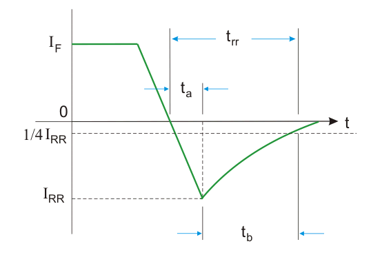
The figure depicts the reverse recovery characteristic of a power diode. Whenever the diode is switched off the current decays from IF to zero and further continues in reverse direction owing to the charges stored in the space charge region and the semiconductor region.
This reverse current attains a peak IRR and again starts approaching zero value and finally, the diode is off after time trr.
This time is defined as reverse recovery time and is defined as the time between the instant forward current reaches zero and the instant the reverse current decays to 25% of IRR. After this time the diode is said to attain its reverse blocking capability.
From the figure above, we see that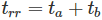
ta → time when charge from depletion region is removed
tb → time when charge from semiconductor region is removed
Also from the figure, we can say that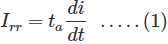
Where,  is the rate of change of reverse current.
The area bounded by the triangular region in the above figure represents the total charge stored or reverse recovery charge, QR. Hence we can write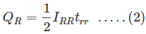
Now, for  , putting in eq.1 and combining with eq.2, we get
Putting eq.3 in eq.1 for , we get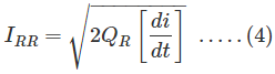
From eq. 3 and 4 we can see that trr and IRR depend on QR which in turn depends upon the initial forward diode current IF.
Another interesting parameter is defined for power diodes from its turn-off characteristics known as Softness Factor (S-factor) defined as the ratio of times tb and ta.
Hence,
If a diode has S-factor equals to unity it is known as a soft-recovery diode and for S-factor less that unity it is known as fast or snappy-recovery diodes.
S-factor indirectly indicates the voltage transient that occurs upon the turn off of the diode. Low S-factor implies high transient overvoltage while high S-factor implies low oscillatory reverse voltage.
The total power loss during turn off is the product of diode current and voltage during trr. Most of the power loss occurs during tb.
In a typical datasheet of power diodes the most important parameters given are IF avg, IF RMS, VRRM, I2t rating, junction temp TJ, trr, S-factor, IRR. Apart from these many other parameters and graphs are also provided.
The power diodes can be classified into the following categories, summarized in the table below, as per their properties:
| Type | Voltage ratings (VRRM) | Current ratings (IF) | Reverse recovery time (trr) | Applications | Remarks |
| General Purpose Diodes | 50-5000 V | 1A to several thousand Amps | ~25µs | UPS, battery chargers, welding, traction, etc. | – |
| Fast Recovery Diode | 50-3000 V | 1A to several thousand Amps | <5µs | SMPS, commutation circuits, choppers, induction heating | Doping is done using platinum or gold |
| Schottky Diodes | Up to 100V | 1-300 A | ~ns | Very high frequency switching power supplies and instrumentation | Metal-semiconductor junction, usually Al-Si(n-type), majority carrier device, hence very low turn off time |
I really enjoyed reading your electrical articles, and I have gained a lot. I will like to receive electrical articles on power electronics as my M.sc. research is on power electronics.
Thank you.