- JFET Definition: A JFET is a type of transistor that controls current flow using an electric field.
- Gate Cut Off Voltage: The voltage where the drain current becomes zero, crucial for both n-channel and p-channel JFETs.
- Shorted Gate Drain Current (IDSS): Maximum current through the JFET when the gate is grounded and VDS is increased.
- Transconductance: The ratio of change in drain current to change in gate-source voltage, vital for understanding JFET performance.
- Dynamic Output Resistance: The ratio of change in drain-source voltage to the change in drain current, indicating how the JFET responds to voltage changes.
During purchasing a JFET for a particular application we need to check the specifications of the device. These specifications are provided by manufacturers. The followings are the parameters used to specify a JFET and these are
- Gate Cut Off Voltage (VGS(off))
- Shorted Gate Drain Current (IDSS)
- Transconductance (gmo)
- Dynamic Output Resistance (rd)
- Amplification Factor (μ)
Gate Cut Off Voltage
At a fixed drain voltage, the drain current (ID) of a JFET depends on the gate to source voltage (VGS). If the gate to source voltage decreases from zero in n channel JFET, the drain current also gets decreased accordingly. The relation between gate to source voltage and drain current is given below. 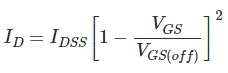 After a certain gate to source voltage (VGS), the drain current ID becomes zero. This voltage is known as Cut Off Gate Voltage (VGS(off)). This voltage numerically equals the pinch-off drain to source voltage (Vp). In the case of p channel JFET if we increase the gate terminal voltage from zero the drain current gets decreased and after a certain gate to source voltage, the drain current becomes zero. This voltage is the cut off gate voltage for p channel JFET. It is the gate cut off voltage for p channel JFET.
Shorted Gate Drain Current
When the gate terminal is grounded (VGS = 0) and the drain-source voltage (VDS) is slowly increased in an n-channel JFET, the drain current increases linearly. After the pinch-off voltage (Vp), the drain current stays constant, reaching its maximum value. This maximum current, called the Shorted Gate Drain Current (IDSS), is fixed for each JFET.
Transconductance
Transconductance is the ratio of change in drain current (δID) to change in the gate to source voltage (δVGS) at a constant drain to source voltage (VDS = Constant).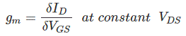
This value is maximum at VGS = 0. This is denoted by gmo. This maximum value (gmo) is specified in a JFET data sheet. The transconductance at any other value of gate to source voltage (gm) can be determined as follows. The expression of drain current (ID) is
By partial differentiating the expression of drain current (ID) in respect of gate to source voltage (VGS)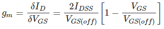
At VGS = 0, the transconductance gets its maximum value and that is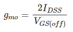
Therefore, we can write,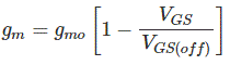
Dynamic Output Resistance
This is the ratio of change of drain to source voltage (δVDS) to the change of drain current (δID) at a constant gate to source voltage (VGS = Constant). The ratio is denoted as rd.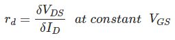
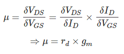
Amplification Factor
The amplification factor is defined as the ratio of change of drain voltage (δVDS) to change of gate voltage (δVGS) at a constant drain current (ID = Constant).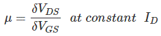
There is a relation between transconductance (gm) and dynamic output resistance (rd) and that can be established in the following way.