

- Boost Converter Definition: A boost converter (step-up chopper) is a device that increases the input DC voltage to a higher output DC voltage.
- Circuit Components: The boost converter circuit includes an inductor, switch, diode, capacitor, and load, each playing a vital role in its operation.
- PWM Control: Pulse Width Modulation (PWM) controls the switching in the converter, with time-based PWM preferred for its simplicity and constant frequency.
- Modes of Operation: The converter operates in two modes—Mode I (switch on, diode off) and Mode II (switch off, diode on)—to store and release energy.
- Duty Cycle: The duty cycle impacts the voltage output, with values above 0.7 leading to instability in practical applications.
DC-DC converters are also known as Choppers. Here we will have a look at the Step Up Chopper or Boost converter which increases the input DC voltage to a specified DC output voltage. A typical Boost converter is shown below.
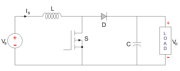
The input voltage source connects to an inductor. A solid-state switch is connected across the source. Another switch, a diode, connects to a capacitor and the load, with these components arranged in parallel.
The inductor connected to input source leads to a constant input current, and thus the Boost converter is seen as the constant current input source. And the load can be seen as a constant voltage source. The controlled switch is turned on and off by using Pulse Width Modulation(PWM). PWM can be time-based or frequency based. Frequency-based modulation has disadvantages like a wide range of frequencies to achieve the desired control of the switch which in turn will give the desired output voltage. Time-based Modulation is mostly used for DC-DC converters. It is simple to construct and use. The frequency remains constant in this type of PWM modulation. The Boost converter has two modes of operation. The first mode is when the switch is on and conducting.
Mode I : Switch is ON, Diode is OFF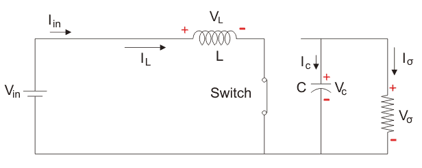
The Switch is ON and therefore represents a short circuit ideally offering zero resistance to the flow of current so when the switch is ON all the current will flow through the switch and back to the DC input source. Let us say the switch is on for a time TON and is off for a time TOFF. We define the time period, T, as  and the switching frequency,
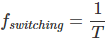
Let us now define another term, the duty cycle, 
Let us analyze the Boost converter in steady state operation for this mode using KVL.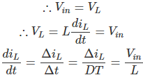
Since the switch is closed for a time TON = DT we can say that Δt = DT.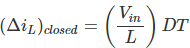
While performing the analysis of the Boost converter, we have to keep in mind that
- The inductor current is continuous and this is made possible by selecting an appropriate value of L.
- The inductor current in steady state rises from a value with a positive slope to a maximum value during the ON state and then drops back down to the initial value with a negative slope. Therefore the net change of the inductor current over anyone complete cycle is zero.
Mode II : Switch is OFF, Diode is ON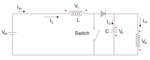
In this mode, the polarity of the inductor is reversed. The energy stored in the inductor is released and is ultimately dissipated in the load resistance, and this helps to maintain the flow of current in the same direction through the load and also step-up the output voltage as the inductor is now also acting as a source in conjunction with the input source. But for analysis, we keep the original conventions to analyze the circuit using KVL.
Let us now analyse the Boost converter in steady state operation for Mode II using KVL.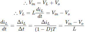
Since the switch is open for a time  we can say that
  .
.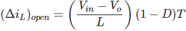
It is already established that the net change of the inductor current over any one complete cycle is zero.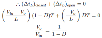
The duty cycle (D) varies between 0 and 1. If D = 1, the output voltage would theoretically be infinite, which isn’t possible. In practice, a duty cycle above 0.7 can cause instability in the Boost converter. Below is a circuit diagram of a Boost converter with an inductance (L) of 20mH, capacitance (C) of 100µF, a 20Ω resistive load, a 1 kHz switching frequency, a 100V DC input, and a duty cycle of 0.5.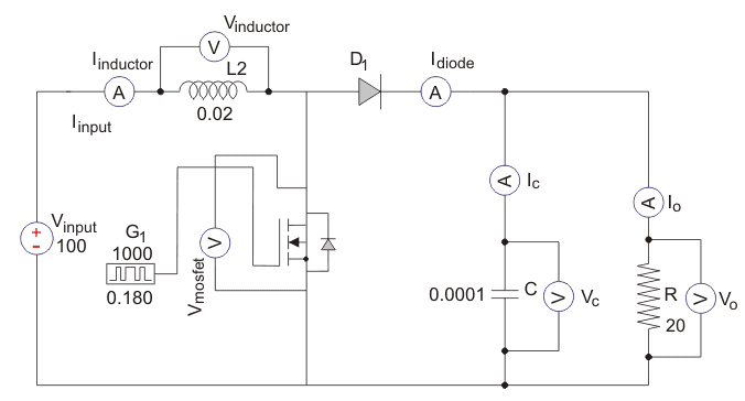
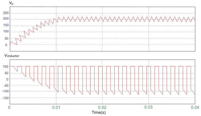
The voltage waveforms are as shown above and the current waveforms are as shown in the figure below.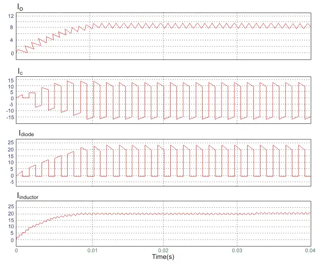
thank you love the information
No problem Fiona, we’re very happy to hear you found the information useful.