- JFET Biasing Definition: JFET biasing involves setting the correct voltage levels at the gate and drain to control the transistor’s operation.
- Pinch-Off Voltage: The pinch-off voltage is the drain voltage at which the depletion layers in a JFET meet, stopping the increase in drain current.
- Gate Cut-Off Voltage: The gate cut-off voltage is the negative voltage at which the JFET drain current drops to zero, crucial for determining the operating range.
- Self-Biasing Method: Self-biasing uses a resistor at the source terminal to create a voltage drop, establishing the proper gate-source voltage.
- Voltage Divider Biasing: This method uses resistors to divide the voltage and set the gate voltage, ensuring the JFET operates correctly within its parameters.
Before discussing JFET biasing, let’s understand what pinch-off voltage is, as it plays a crucial role in determining the biasing level of a JFET.
Pinch Off Voltage
In an n-channel JFET, applying a positive potential at the drain while keeping the source grounded causes current to flow from drain to source. This creates a voltage drop along the channel, with higher potential near the drain than the source. If the gate is grounded, the PN junction between the gate and channel is reverse biased, with a wider depletion layer near the drain than the source.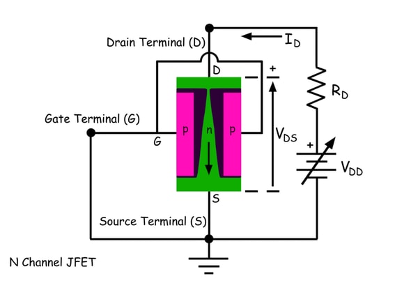
As we continuously increase the drain voltage, the depletion layer width increases more near the drain than the source. At a certain drain voltage, the depletion layers meet, known as the pinch-off voltage. At zero gate voltage, this is the drain voltage where the depletion layers touch. Before pinch-off, drain current increases linearly with drain-source voltage, becoming almost constant just after pinch-off. Further increasing the drain voltage beyond pinch-off keeps the current constant until avalanche breakdown occurs at a higher voltage, rapidly increasing the current. Therefore, a JFET must operate between pinch-off and breakdown voltages for amplification. To maintain this range, a DC voltage source or battery is connected in series with the load resistance.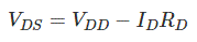
The pinch-off voltage appears between drain and source is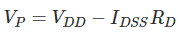 Here IDSS is the drain current flowing through the channel at pinch-off while the gate terminal is in ground potential.
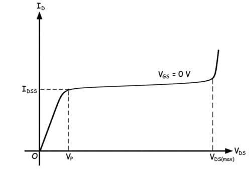
In an n-channel JFET, applying a negative potential to the gate terminal further increases the depletion layer width between the gate region and channel. This increases the reverse biasing of the junction. As discussed earlier, with the drain voltage applied and the gate grounded, the depletion layers near the drain touch, creating a small channel opening for the drain current to flow.
When we increase the negative potential of the gate terminal, the channel opening gets narrower and hence drain current gets reduced. If we go on increasing negative gate terminal voltage, the drain current continues decreasing, and it would be seen that the drain current becomes zero at a certain gate voltage. This voltage is known as gate cut off voltage. The value of the gate cut off voltage is equal to pinch off voltage of a junction field effect, but the polarity of these two voltages are opposite. 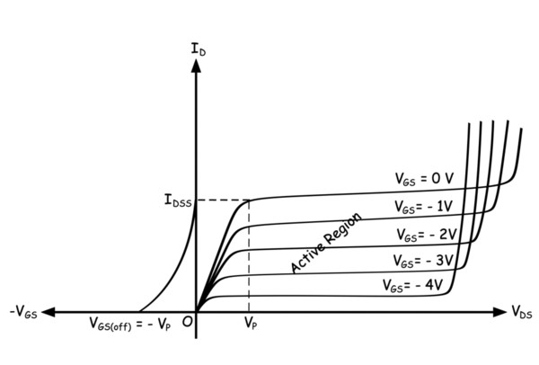
So the operating range of the input signal of a JFET should be 0 to – VGS(off) where VGS(off) is the gate cut off voltage. To ensure the operating range of varying input signal the gate circuit must be associated with a fixed biased voltage which can be applied to the gate circuit either by a separate battery source or by voltage diversion from the output circuit. Depending on the applied methods, gate biasing of a JFET can be of three types.
Biasing of JFET by a Battery at Gate Circuit
This is done by inserting a battery in the gate circuit. The negative terminal of the battery is connected to the gate terminal. As the gate current in JFET is almost zero, there would be no voltage drop across the input gate resistance. Hence the negative potential of the battery directly reaches to gate terminal. The corresponding drain current and drain to source voltage would be the output operating point of the transistor.
NB: – Here in all biasing circuits below, we have included the input AC signal for the better detailing of the circuit, but during calculation of biasing point or operating point of the JFET, we will ignore the AC signal as the biasing only deals with DC.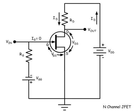 As, in JFET there is no gate current,
 We can find the value of drain current ID from the relation given below as IDSS and VGS(off) (= – VP) are given in transistor data sheet.
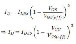 The value of VDS can be found by applying KVL at output circuit
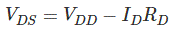
The operating point of the JFET is located at the coordinate (VDS, ID) on the characteristic graph.
Self Biasing of a JFET
Here one resistance RS is inserted between source terminal and ground.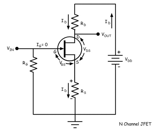 The voltage across RS would be
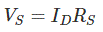
Here the gate terminal is also grounded through a resistance RG. As there is no gate current, zero ground potential appears at the gate terminal.
The voltage between the gate and source is VGS.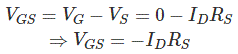 This equation tells us that here the gate terminal always gets negative potential than the source terminal.
  After determining the value of ID, and VDS from above relation, we can put the operating point on the characteristic graph at the coordinate (VDS, ID).
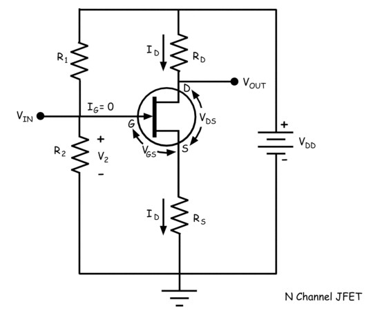
Voltage Divider Biasing of a JFET
Two series connected resistors form a voltage divider circuit. The voltage at the gate terminal can be calculated by voltage division rule. In this way, the applied drain voltage is utilized to get the gate terminal voltage. A resistance is inserted into source terminal in series. The device current flows through the resistance and causes a voltage drop. If this source voltage drop is greater than voltage appears at the gate terminal, the gate to source voltage has a negative value which is desired for JFET operation. Let us consider the following circuit.