

- PNP Transistor Definition: A PNP transistor is defined as a bipolar junction transistor with an N-type semiconductor sandwiched between two P-type semiconductors.
- Current Flow Direction: In a PNP transistor, the current flows from the Emitter to the Collector.
- Working Principle: The PNP transistor works by using holes as the main charge carriers, requiring a Base voltage that is more negative than the Emitter.
- Symbol of PNP Transistor: The symbol includes an arrow on the Emitter showing the direction of conventional current flow.
- PNP Transistor Switch: It acts as a switch, turning ON when the Base voltage is sufficiently negative compared to the Emitter voltage.
What is a PNP Transistor
A PNP transistor is a bipolar junction transistor constructed by sandwiching an N-type semiconductor between two P-type semiconductors. A PNP transistor has three terminals – a Collector (C), Emitter (E) and Base (B). The PNP transistor behaves like two PN junctions diodes connected back to back.
These back to back PN junction diodes are known as the collector-base junction and base-emitter junction.
The three terminals of the PNP transistor are the Emitter, Collector, and Base. The Emitter supplies charge carriers to the Collector through the Base. The Base controls and regulates the current flow from the Emitter to the Collector.
The equivalent circuit of a PNP transistor is as shown in the figure below.

PNP Transistor Symbol and Construction
The construction of a PNP transistor is similar to an NPN transistor. In an NPN transistor, a P-type semiconductor is sandwiched between two N-type semiconductors. In a PNP transistor, an N-type semiconductor is sandwiched between two P-type semiconductors.
The construction of the PNP Transistor is as shown in the below figure.


In P-type semiconductors, the majority charge carriers are holes. Therefore, in the PNP transistor, the formation of the current is due to the movement of holes.
The middle N-type layer is the Base terminal (B). The left P-type layer is the Emitter terminal (E), and the right P-type layer is the Collector terminal (C).
The Emitter and Collector (P-type) layers are heavily doped compared to the Base (N-type) layer. Therefore, the depletion region at both junctions is more penetrate towards the Base layer. The area of the Emitter and Collector layer is more compared to the Base layer.
In N-type semiconductors, a large number of free electrons are available. But, the width of the middle layer is very small and it is lightly doped. So significantly less free electrons are present in the Base region.
The symbol of the PNP transistor is as shown in the below figure. The arrowhead shows that the current will flow through Emitter to Collector.

How Does a PNP Transistor Work
The positive terminal of a voltage source (VEB) is connected with Emitter (P-type) and the negative terminal is connected with the Base terminal (N-type). Therefore, the Emitter-Base junction is connected in forward bias.
And the positive terminal of a voltage source (VCB) is connected with the Base terminal (N-type) and the negative terminal is connected with the Collector terminal (P-type). Hence, the Collector-Base junction is connected in reverse bias.

Due to this type of bias, the depletion region at Emitter-Base junction is narrow, because it is connected in forward bias. While the Collector-Base junction is in reverse bias and hence the depletion region at Collector-Base junction is wide.
The Emitter-Base junction is forward biased, allowing many holes from the Emitter to cross into the Base. At the same time, a few electrons from the Base enter the Emitter and recombine with the holes.
The loss of holes in the emitter is equal to the number of electrons present in the Base layer. But The number of electrons in the Base is very small because it is a very lightly doped and thin region. Therefore, almost all holes of Emitter will cross the depletion region and enter into the Base layer.
Because of the movement of holes, the current will flow through the Emitter-Base junction. This current is known as Emitter current (IE). The holes are majority charge carriers to flow the Emitter current.
The remaining holes which do not recombine with electrons in Base, that holes will further travel to the Collector. The Collector current (IC) flows through the Collector-Base region due to holes.
PNP Transistor Circuit
The circuit of the PNP transistor is as shown in the below figure.
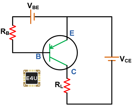
If we compare the circuit of PNP transistor with NPN transistor, then here the polarity and direction of current are reversed.
If a PNP transistor is connected with voltage sources as shown in the above figure, the base current will flow through the transistor. The small amount of base current controls the flow of a large amount of current through emitter to collector provided that the Base voltage is more negative than the Emitter voltage.
If the Base voltage is not more negative than the Emitter voltage, the current cannot flow through the device. So, it is necessary to give a voltage source in reverse bias more than 0.7 V.
Two resistors RL and RB connected in the circuit to limit the maximum amount of current through the transistor.
If you apply a Kirchhoff’s current law (KCL), the emitter current is a summation of the base current and collector current.
![\[ I_E = I_B + I_C \]](https://www.electrical4u.com/wp-content/ql-cache/quicklatex.com-8bb6668aafa712bfce8c6f37d21e210f_l3.png "Rendered by QuickLaTeX.com")
![\[ I_C = I_E - I_B \]](https://www.electrical4u.com/wp-content/ql-cache/quicklatex.com-2b6c7e54c2ad27e85034143850a75618_l3.png "Rendered by QuickLaTeX.com")
PNP Transistor Switch
Generally, when a switch is OFF, current cannot flow, acting as an open circuit. When the switch is ON, current flows through the circuit, acting as a closed circuit.
The transistor is nothing but a power electronics switch that can work like normal switches. Now the question is how can we use PNP transistor as a switch?
As we have seen in the working of the PNP transistor, if the Base voltage is not more negative then Emitter voltage, the current cannot flow through the device. So, Base voltage is a minimum of 0.7 V in reverse bias to conduct the transistor.
It means that, if the Base voltage is zero or less than 0.7 V, the current cannot flow and it acts as an open circuit.

To turn ON the transistor, the Base voltage must more than 0.7 V. In this condition, the transistor acts as a close switch.

PNP vs NPN Transistor
The main differences when comparing PNP transistors vs NPN transistors have been summarized in the table below:
| PNP Transistor | NPN Transistor | |
| Structure | It has one N-type and two P-type semiconductors. | It has two N-type and one P-type semiconductor. |
| Direction of current | The current will flow through the emitter to the collector. | The current will flow through the collector to the emitter. |
| Majority charge carrier | Holes | Electron |
| Minority charge carrier | Electrons | Holes |
| Switching time | Slower | Faster |
| Junction biasing | Emitter-base junction is in reverse bias and collector-base junction is in forward bias. | Emitter-base junction is in forward bias and collector-base junction is in reverse bias. |
| Symbol |  |  |
| Collector-emitter voltage | Negative | Positive |
| Emitter arrow | Pointed in | Pointed out |